Pin configuration, Pin plastic dip (600 mil), shrink dip (400 mil) – NEC PD75402A User Manual
Page 17
6
CHAPTER 1. GENERAL
1.5
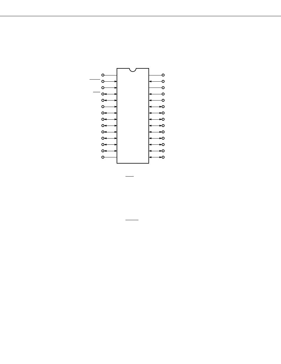
PIN CONFIGURATION
1.5.1
28-Pin Plastic Dip (600 mil), Shrink Dip (400 mil)
(1)
Normal operating mode
P00 to P03
: Port 0
SCK
: Serial clock input/output
P10, P12
: Port 1
SO/SB0
: Serial output/input/output
P20 to P23
: Port 2
SI
: Serial input
P30 to P33
: Port 3
PCL
: Clock output
P50 to P53
: Port 5
INT0
: External vectored interrupt input
P60 to P63
: Port 6
INT2
: External test input
X1, X2
: Oscillator pin
RESET
: Reset input
V
DD
: Power supply
V
SS
: Ground
V
PP
: Externally set to GND potential
NC
: No connection
Remarks
Parentheses for the
µ
PD75P402.
*
If using the
µ
PD75P402 and the printed circuit board commonly in the
µ
PD75402A, the NC pin is to be set to the
GND potential.
(V
PP
) NC
*
RESET
P00
P01/SCK
P02/SO/SB0
P03/SI
P50
P51
P52
P53
P30
P31
P32
V
SS
1
2
3
4
5
6
7
8
9
10
11
12
13
14
16
V
DD
X1
X2
P12/INT2
P10/INT0
P23
P22/PCL
P21
P20
P63
P62
P61
P60
P33
15
17
18
19
20
21
22
23
24
25
26
27
28
µ
PD75402AC/CT-
×××
µ
PD75P402C/CT-CT