NEC PD75402A User Manual
Page 73
62
CHAPTER 5. PERIPHERAL HARDWARE FUNCTIONS
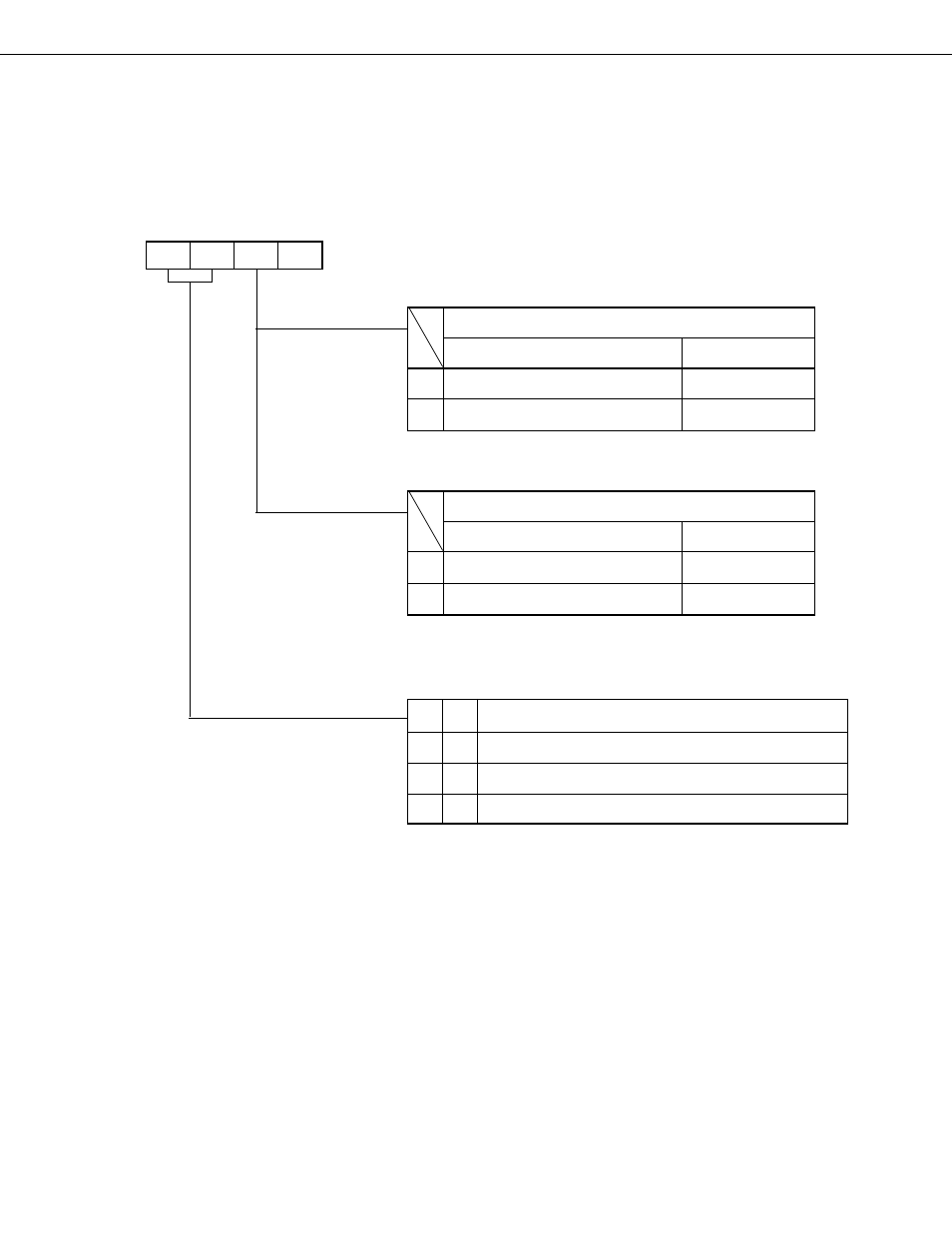
Next, the processor clock control register (PCC) of the
µ
PD75402 is shown below. Setting of bit 1 of the PCC is
performed by a 4-bit memory handling instruction. At this time, ensure that bits 3, 2 and 0 are reset to “0” so that
the pattern “00
×
0” is written.
Fig. 5-17
µ
PD75402 Processor Clock Control Register Format
Note
1. Ensure that 0 is always written to PCC bit 0.
2. Unlike the
µ
PD75402A, in the
µ
PD75402, switching
Φ
is 2-step rather than 3-step. High-speed mode (0.95
µ
s at 4.19 MHz) cannot be specified.
3
2
1
0
Symbol
FB3H
PCC3
PCC2
PCC1
0
PCC
CPU clock selection bits when f
XX
≤
4.19 MHz
( ) : When f
XX
= 4.19 MHz
CPU Clock Frequency
1 Machine Cycle
0
Φ
Output = f
XX
/64 (65.5 kHz)
15.3
µ
s
1
Φ
= f
XX
/8 (524 kHz)
19.1
µ
s
When 4.19 MHz < f
XX
≤
5.0 MHz
( ) : When f
XX
= 4.91 MHz
CPU Clock Frequency
1 Machine Cycle
0
Φ
Output = f
XX
/64 (76.7 kHz)
13
µ
s
1
Φ
= f
XX
/8 (614 kHz)
1.63
µ
s
f
XX
: Main system clock oscillation circuit output frequency
CPU operating mode control bit
0
0
Normal operating mode
0
1
HALT mode
1
0
STOP mode
1
1
Setting prohibited
Address