Unused pin treatment, Notes on use of p00 pin and reset pin – NEC PD75402A User Manual
Page 31

CHAPTER 2. PIN FUNCTIONS
20
V
DD
V
DD
V
DD
V
DD
Diode with
Small V
F
P00, RESET
P00, RESET
2.5
UNUSED PIN TREATMENT
Pin
P00
P01 to P03
P10 and P12
P20 to P23
P30 to P33
P50 to P53
P60 to P63
NC
*
If using the
µ
PD75P402 and the printed circuit board commonly, the NC pins should be connected directly to V
SS
.
2.6
NOTES ON USE OF P00 PIN AND RESET PIN
The P00 and RESET pins are provided with the test mode setting function of test mode (for IC test) which tests
the internal operation of the
µ
PD75402A in addition to the functions described in 2.2.1 and 2.2.8.
When a voltage exceeding V
DD
is applied to either of these pins, the test mode is set. Consequently, if noise
exceeding V
DD
is added even in a normal operation, the test mode is set and the normal operation may not be
continued.
For example, when wires from the P00 pin or RESET pin are long, inter-wiring noise may be added to these pins
and the pin voltage may exceed V
DD
, resulting in a misoperation.
Therefore, wiring should be carried out so that inter-wiring noise is suppressed as far as possible.
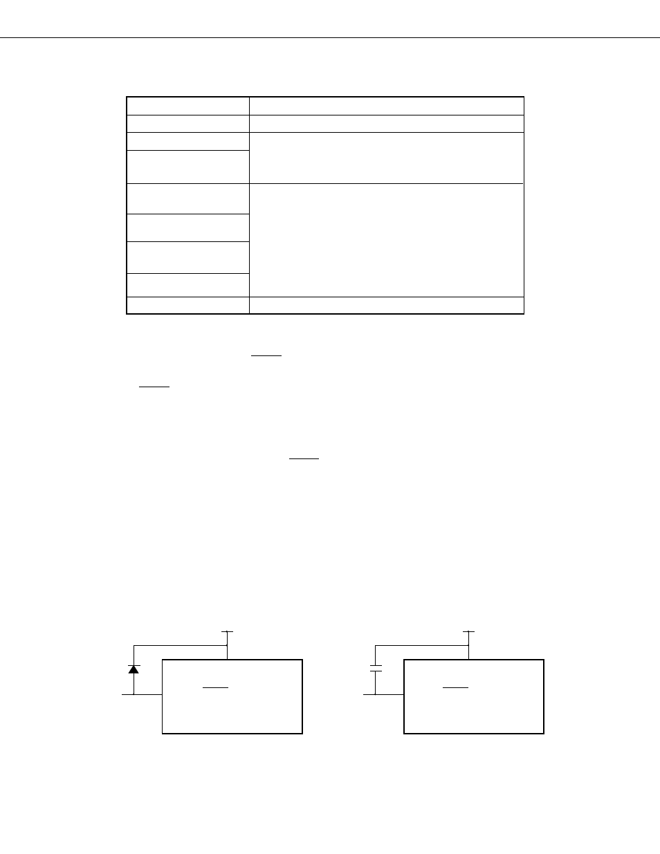
If it is impossible to suppress the noise, noise prevention measures by means of external parts should be taken
as shown below.
o
Insert diode with small
o
Insert capacitor between
V
F
(less than 0.3 V)
V
DD
and P00/RESET pin.
between V
DD
and
P00/RESET pin.
Recommended Connection Method
Connect to V
SS
.
• With pull-up resistor Connect to V
DD
.
• Without pull-up resistor
Connect to V
SS
or V
DD
.
• With pull-up resistor
Input status: Connect to V
DD
.
Output status: Leave open.
• Without pull-up resistor
Input status: Connect to V
SS
to V
DD
.
Output status: Leave open.
Leave open or connect directly to V
SS
.
*
