NEC PD75402A User Manual
Page 158
147
CHAPTER 8. RESET FUNCTION
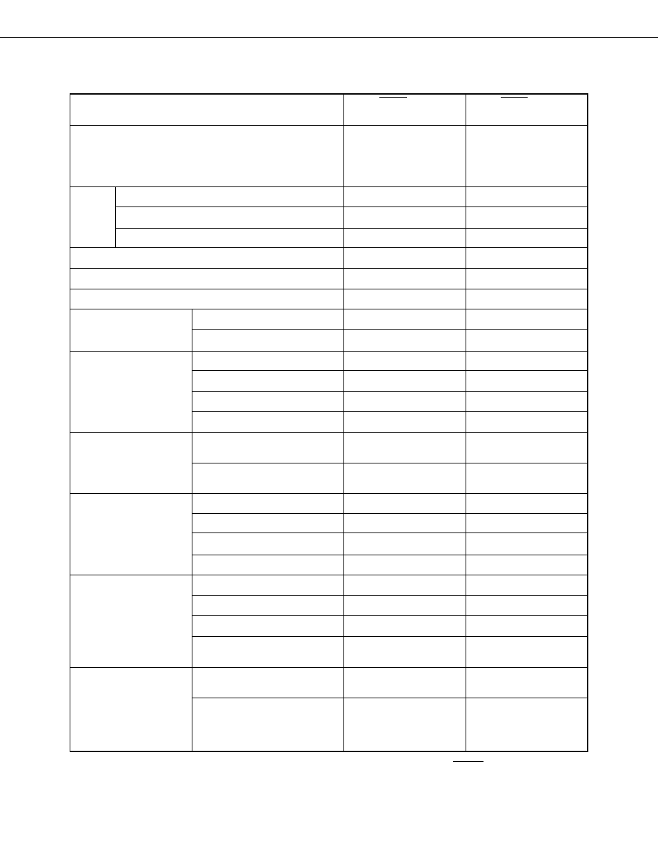
Table 8-1 State of Hardware after Reset
*
The contents of data memory addresses 038H to 03DH are made undefined by RESET input.
Hardware
RESET Input
standby mode
RESET Input
during operation
Program counter (PC)
PSW
Low-order 3 bits of
program memory address
000H set in PC10 to PC8
and contents of address
001H set in PC7 to PC0
Retained
0
0
Undefined
Retained*
Retained
Undefined
0
Retained
0
0
Retained
0
0
Reset (0)
0
0
0
OFF
Clear (0)
0
0
Input
• On-chip pull-up resistor
•••••
High level
• Open-drain
•••••
High impedance
Low-order 3 bits of
program memory address
000H set in PC10 to PC8
and contents of address
001H set in PC7 to PC0
Undefined
0
0
Undefined
Undefined
Undefined
Undefined
0
Undefined
0
0
Undefined
0
0
Reset (0)
0
0
0
OFF
Clear (0)
0
0
Input
• On-chip pull-up resistor
•••••
High level
• Open-drain
•••••
High impedance
Carry flag (CY)
Skip flag (SK0 to SK2)
Interrupt status flag (IST0)
Stack pointer (SP)
Data Memory (RAM)
General register (X, A, H, L)
Basic interval timer
Serial interface
Clock generator,
clock output circuit
Counter (BT)
Mode register (BTM)
Shift register (SIO)
Operation mode register (CSIM)
SBI control register (SBIC)
Slave address register (SVA)
Processor clock control register
(PCC)
Clock output mode register
(CLOM)
Interrupt request flag (IRQ
×××
)
Interrupt enable flag (IE
×××
)
Interrupt master enable flag (IME)
INT0 mode register (IM0)
Output buffer
Output latch
I/O mode register (PMGA, PMGB)
Pull-up resistor specification
register (POGA)
Pin state P00 to P03, P10, P12, P20
to P23, P30 to P33, P60 to P63
P50 to P53
Digital input/output port
Pin state
Interrupt function