NEC PD75402A User Manual
Page 112

101
CHAPTER 5. PERIPHERAL HARDWARE FUNCTIONS
(3)
Register setting
When the device is used in the SBI mode, setting can be performed by means of the following two registers:
• Serial operating mode register (CSIM)
• Serial bus interface control register (SBIC)
(a)
Serial operating mode register (CSIM)
When the SBI mode is used, CSIM is set as shown below (see 5.5.3 (1) “Serial operating mode register”
for full details of CSIM).
CSIM is manipulated by 8-bit manipulation instructions. Bit manipulation of bits 7, 6 and 5 is also possible.
Reset input clears the CSIM register to 00H.
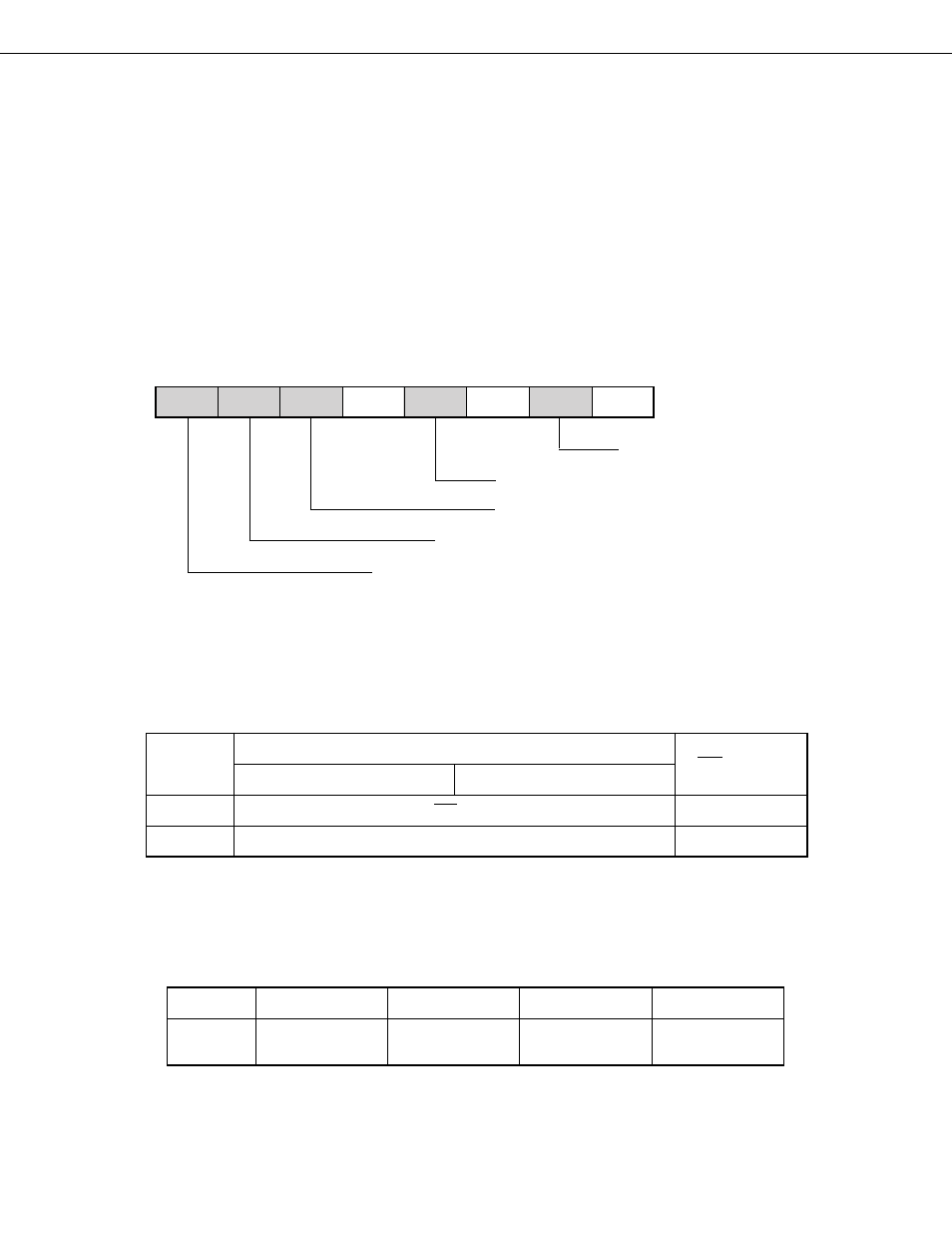
The shaded area indicates bits used in the SBI mode.
Address
7
6
5
4
3
2
1
0
Symbol
FE0H
CSIE
COI
WUP
0
CSIM3
0
CSIM1
0
CSIM
Serial Clock Selection Bit (W)
Serial Interface Operating Mode Selection Bit (W)
Wake-up Functing Specification Bit (w)
Signal from Address Comparator (R)
Serial Interface Operation Enable/Disable Specification Bit (W)
Remarks
(R)
Read only
(W)
Write only
Serial clock selection bit (W)
Serial Clock
CSIM1
SCK Pin Mode
3-Wire Serial I/O Mode
SBI Mode
0
Input clock to SCK pin from off chip
Input
1
f
XX
/2
4
(262 kHz)
Output
Remarks
Figure in ( ) apply to f
XX
= 4.19 MHz operation
Serial interface operating mode selection bit (W)
Shift Register
Bit Order
CSIM3
Operating Mode
SO Pin Function
SI Pin Function
1
SBI mode
SIO
7 to 0
↔
XA
(MBS-first transfer)
SB0/P02
(N-ch open-drain
input/output)
P03 input
