NEC PD75402A User Manual
Page 54
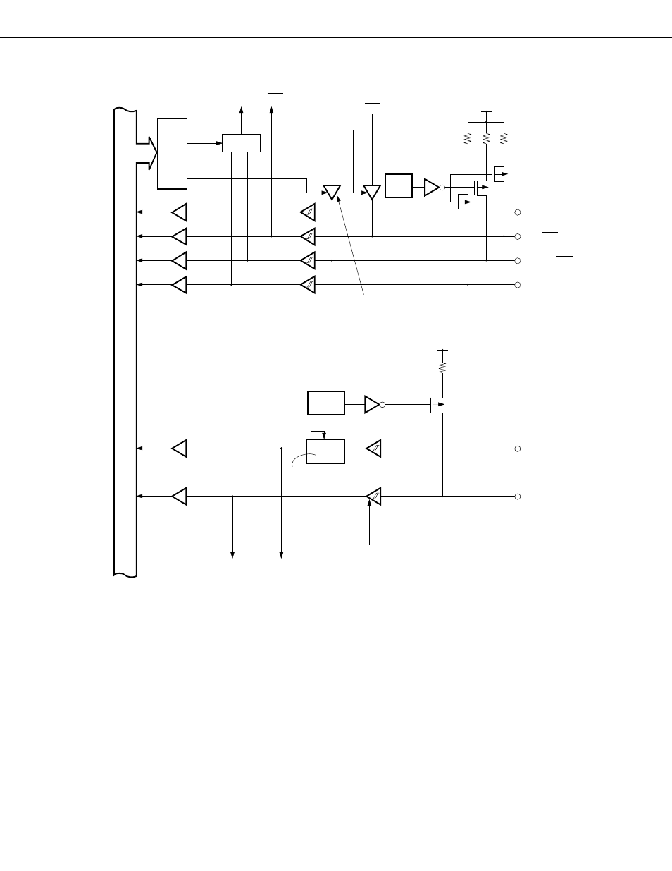
43
CHAPTER 5. PERIPHERAL HARDWARE FUNCTIONS
Fig. 5-2 Configuration of Ports 0 and 1
Input Buffer
Internal Bus
Input Buffer
or f
XX
/64
Noise Elimination Circuit
Input Buffer with
Hysteresis Characteristics
INT0
INT2
P12/INT2
P10/INT0
P-ch
Pull-Up
Resistor
PO0
POGA
Bit 0
V
DD
Output Buffer with Capability
of Switching between Push-Pull
Output and N-ch Open-Drain Output
P03/SI
P02/SO/SB0
P01/SCK
P00
P-ch
Pull-Up
Resistors
V
DD
SI
SCK
SO
Internal
SCK
Selcetor
CSIM
PO1
POGA
Bit 1
Φ
This manual is related to the following products: