Data memory (ram) – NEC PD75402A User Manual
Page 44

CHAPTER 4. INTERNAL CPU FUNCTIONS
33
4.3
DATA MEMORY (RAM)
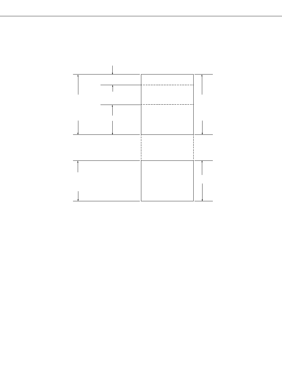
The data memory consists of the data and peripheral hardware areas as shown in Fig. 4-3.
Fig. 4-3 Data Memory Map
(1)
Data area
The
µ
PD75402A’s data area consists of the static RAM (64 words
×
4 bits). The data area is used to store processing
data and is operated by the memory manipulation instruction.
The static RAM is mapped to Memory bank 0 by 64
×
4 bits. While Bank 0 is mapped as the data area, it is also
available as the general register area (000H to 003H) and the stack area (020H to 03FH).
In the static RAM, 1 address consists of 4 bits. It is possible either to operate per 8 bits by the 8-bit memory
manipulation instruction or to operate per bit by the bit manipulation instruction, however. In the 8-bit manipulation
instruction, an even address should be specified.
• General register area
Operation is possible either by the general register manipulation instruction or by the memory manipulation
instruction. Up to four 4-bit registers are available. Of the 4 general registers, that part which is not used in the
program is available as the data area (see 4.4 “GENERAL REGISTER”).
• Stack area
The stack area is set by an instruction and is available as the save area at the subroutine or interrupting process
execution (see 4.6 “STACK POINTER”). In that case, the stack area is at the static RAM’s addresses 020H to 03FH.
Data Memory
Memory Bank
Bank 0
(64
Ч
4)
(4
Ч
4)
(32
Ч
4)
128
Ч
4
Not built in.
0 0 0 H
0 0 3 H
0 0 4 H
0 2 0 H
0 3 F H
F 8 0 H
F F F H
General
Register Area
Data Area
Static RAM
(64
×
4)
Bank 15
Stack Area
Peripheral
Hardware
Area
