NEC PD75402A User Manual
Page 123
112
CHAPTER 5. PERIPHERAL HARDWARE FUNCTIONS
(6)
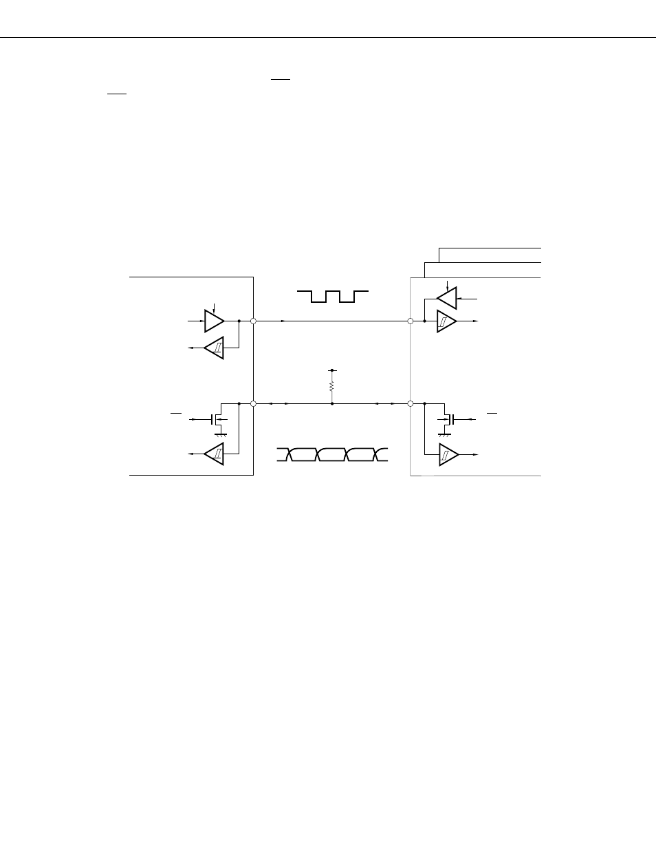
Pin configuration
The configuration of the serial clock pin (SCK) and the serial data bus pin SB0 is as shown below.
(a)
SCK .................... Pin for input/output of serial clock
➀
Master ........ CMOS, push-pull output
➁
Slave ........... Schmitt input
(b) SB0 .................... Serial data input/output dual- function pin
For both master and slave, output is N-ch open-drain, input is Schmitt input.
Since the serial data bus line output is N-ch open-drain, an external pull-up resistor is necessary.
Fig. 5-48 Pin Configuration Diagram
Note
Since the N-ch open drain must be turned off during data reception, FFH should be written to SIO
beforehand. It can always be turned off during transmission.
However, when the wake-up function specification bit (WUP) is 1, the N-ch transistor is always off, and
therefore FFH need not be written to SIO prior to reception.
Slave Device
(Clock Output)
Clock Input
SO
SI
N-ch Open Drain
SB0
R
L
Serial Data Bus
SB0
Serial Clock
Master Device
Clock Output
(Clock Input)
N-ch Open Drain
SO
SI