Input or output cycles, Figure 6, Memory read or write cycle – Zilog Z08470 User Manual
Page 22: E the, Input or out, Put cycles
Architectural Overview
UM008007-0715
10
Z80 CPU
User Manual
Input or Output Cycles
Figure 7 shows an I/O read or I/O write operation. During I/O operations, a single wait
state is automatically inserted. The reason for this single wait state insertion is that during
I/O operations, the period from when the IORQ signal goes active until the CPU must
sample the WAIT line is short. Without this extra state, sufficient time does not exist for an
I/O port to decode its address and activate the WAIT line if a wait is required. Addition-
ally, without this wait state, it is difficult to design MOS I/O devices that can operate at
full CPU speed. During this wait state period, the WAIT request signal is sampled.
During a read I/O operation, the RD line is used to enable the addressed port onto the data
bus, just as in the case of a memory read. The WR line is used as a clock to the I/O port for
write operations.
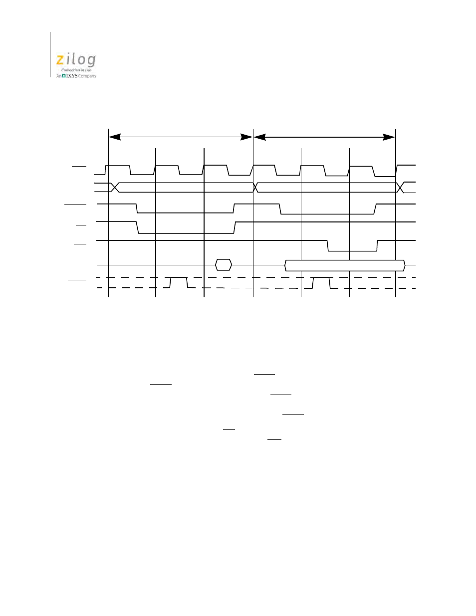
Figure 6. Memory Read or Write Cycle
CLK
D7–D0
A15 –A0
MREQ
RD
WAIT
WR
Memory Address
Memory Address
T2
T3
T1
T2
T3
In
Memory Read Cycle
Memory Write Cycle
Data Out