Architectural overview, Figure 1, Z80 cpu block diagram – Zilog Z08470 User Manual
Page 13
UM008007-0715
Architectural Overview
Z80 CPU
User Manual
1
Architectural Overview
Zilog’s Z80 CPU family of components are fourth-generation enhanced microprocessors
with exceptional computational power. They offer higher system throughput and more
efficient memory utilization than comparable second and third-generation microproces-
sors. The speed offerings from 6–20 MHz suit a wide range of applications which migrate
software. The internal registers contain 208 bits of read/write memory that are accessible
to the programmer. These registers include two sets of six general-purpose registers which
can be used individually as either 8-bit registers or as 16-bit register pairs. In addition,
there are two sets of Accumulator and Flag registers.
The Z80 CPU also contains a Stack Pointer, Program Counter, two index registers, a
refresh register, and an interrupt register. The CPU is easy to incorporate into a system
because it requires only a single +5V power source. All output signals are fully decoded
and timed to control standard memory or peripheral circuits; the Z80 CPU is supported by
an extensive family of peripheral controllers.
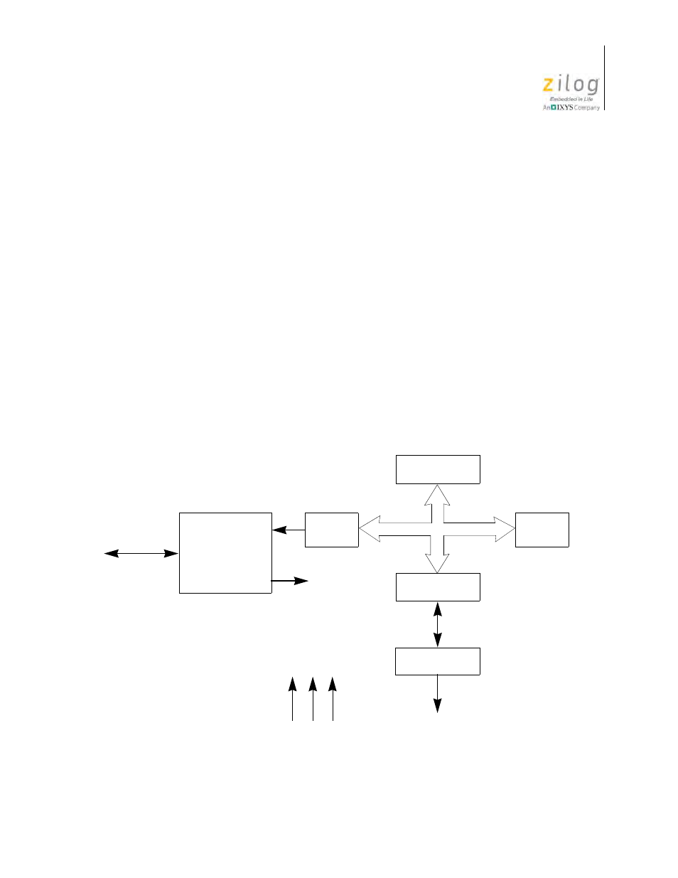
Figure 1 shows the internal architecture and major elements of the Z80 CPU.
Figure 1. Z80 CPU Block Diagram
13
CPU and
System
Control
Signals
Inst.
Register
Data Bus
Control
Internal Data Bus
CPU
Registers
ALU
CPU
Control
Address
Control
16-Bit
Address Bus
+5V GND CLK
I
n