Instruction fetch, Figure 4, Basic cpu timing example – Zilog Z08470 User Manual
Page 20
Architectural Overview
UM008007-0715
8
Z80 CPU
User Manual
WAIT state is entered during the following cycle. Using this technique, the read can be
lengthened to match the access time of any type of memory device. See the
section on page 10 to learn more about the automatic WAIT state.
Instruction Fetch
Figure 5 depicts the timing during an M1 (op code fetch) cycle. The Program Counter is
placed on the address bus at the beginning of the M1 cycle. One half clock cycle later, the
MREQ signal goes active. At this time, the address to memory has had time to stabilize so
that the falling edge of MREQ can be used directly as a chip enable clock to dynamic
memories. The RD line also goes active to indicate that the memory read data should be
enabled onto the CPU data bus. The CPU samples the data from the memory space on the
data bus with the rising edge of the clock of state T3, and this same edge is used by the
CPU to turn off the RD and MREQ signals. As a result, the data is sampled by the CPU
before the RD signal becomes inactive. Clock states T3 and T4 of a fetch cycle are used to
refresh dynamic memories. The CPU uses this time to decode and execute the fetched
instruction so that no other concurrent operation can be performed.
During T3 and T4, the lower seven bits of the address bus contain a memory refresh
address and the RFSH signal becomes active, indicating that a refresh read of all dynamic
memories must be performed. To prevent data from different memory segments from
being gated onto the data bus, an RD signal is not generated during this refresh period. The
MREQ signal during this refresh period should be used to perform a refresh read of all
memory elements. The refresh signal cannot be used by itself, because the refresh address
is only guaranteed to be stable during the MREQ period.
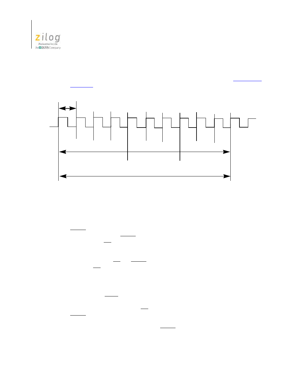
Figure 4. Basic CPU Timing Example
CLK
T Cycle
Machine Cycle
M1
(Opcode Fetch)
Instruction Cycle
M2
(Memory Read)
M3
(Memory Write)
T1
T1
T1
T2
T2
T2
T3
T3
T3