Altera RapidIO II MegaCore Function User Manual
Page 171
Chapter 6: Software Interface
6–33
Transport and Logical Layer Registers
August 2014
Altera Corporation
RapidIO II MegaCore Function
User Guide
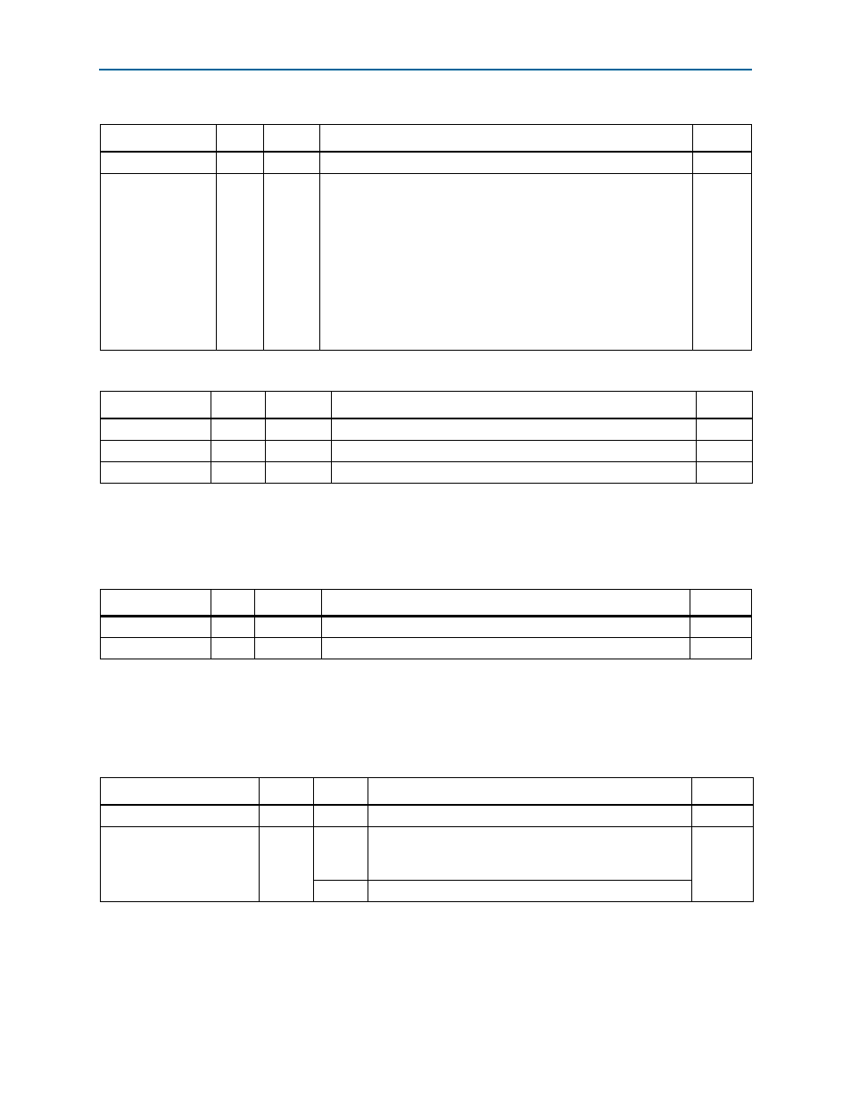
Table 6–33. Processing Element Logical Layer Control CSR—Offset: 0x4C
Field
Bits
Access
Function
Default
RSRV
[31:3]
RO
Reserved
29'h0
EXT_ADDR_CTRL
[2:0]
RO
Controls the number of address bits generated by the Processing
element as a source and processed by the Processing element as the
target of an operation.
3'b100 – Processing element supports 66 bit addresses
3'b010 – Processing element supports 50 bit addresses
3'b001 – Processing element supports 34 bit addresses
All other values are reserved.
The RapidIO II IP core supports only 34-bit addresses, so the value of
this field is always 3’b001.
3'b001
Table 6–34. Local Configuration Space Base Address 0 CSR—Offset: 0x58
Field
Bits
Access
Function
Default
RSRV
[31]
RO
Reserved
1'b0
LCSBA
[30:15]
RO
Reserved for a 34-bit local physical address
16'h0
LCSBA
[14:0]
RO
Reserved for a 34-bit local physical address
15'h0
Note to
:
(1) The Local Configuration Space Base Address 0 register is hard coded to zero. If the Input/Output Avalon-MM master interface is connected to
the Register Access Avalon-MM slave interface, regular read and write operations rather than MAINTENANCE operations can be used to access
the processing element's registers for configuration and maintenance.
Table 6–35. Local Configuration Space Base Address 1 CSR—Offset: 0x5C
Field
Bits
Access
Function
Default
LCSBA
[31]
RO
Reserved for a 34-bit local physical address
1'b0
LCSBA
[30:0] RW
Bits [33:4] of a 34-bit physical address
31'h0
Note to
:
(1) This register holds the local physical address double-word offset of the processing element’s configuration register space. If the Input/Output
Avalon-MM master interface is connected to the Register Access Avalon-MM slave interface then regular read and write operations, rather than
MAINTENANCE
operations, can be used to access the processing element's registers for configuration and maintenance, based on this address.
User logic must write the correct offset value in this register to ensure that these read and write operations can work correctly.
Table 6–36. Base Device ID CSR—Offset: 0x60 (Part 1 of 2)
Field
Bits
Access
Function
Default
RSRV
[31:24]
RO
Reserved
8'h0
Base_deviceID
[23:16]
RW
This is the base ID of the device in a small common
transport system. The value of this field appears on the
base_device_id
output signal.
8'hFF
RO
Reserved if the system does not support 8-bit device ID.