Altera RapidIO II MegaCore Function User Manual
Page 142
6–4
Chapter 6: Software Interface
Memory Map
RapidIO II MegaCore Function
August 2014
Altera Corporation
User Guide
0x4C
Processing Element Logical
Layer
Control
RapidIO Interconnect Specification v2.2 Part 1:
Input/Output Logical Specification
0x58
Local
Configuration Space Base
Address 0
0x5C
Local
Configuration Space Base
Address 1
0x60
Base
Device ID
RapidIO Interconnect Specification Part 3: Common
Transport Specification
0x68
Host
Base Device ID Lock
0x6C
Component
Tag
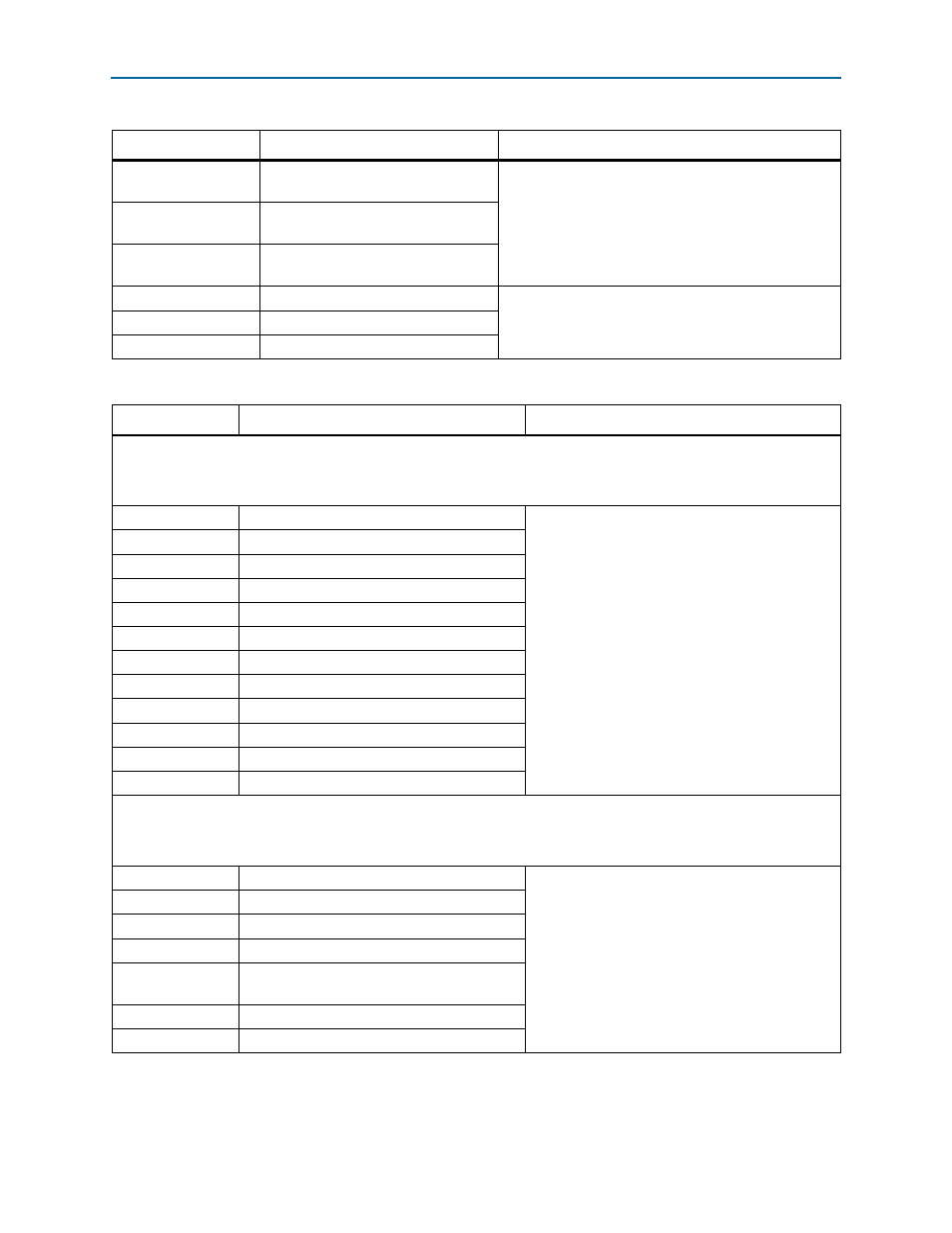
Table 6–3. CAR and CSR Memory Map (Part 2 of 2)
Address
Name
Register Specification Available in
Table 6–4. Extended Features and Implementation-Defined Registers Memory Map (Part 1 of 3)
Address
Name
Used by Module
Extended Features Space: LP-Serial
These registers are defined in RapidIO Interconnect Specification v2.2 Part 6: LP-Serial Physical Layer Specification and
described in
“Physical Layer Registers” on page 6–6
0x100
LP-Serial Register
Block Header
Physical layer
0x104–0x11C
Reserved
0x120
Port
Link Time-out Control
0x124
Port
Response Time-out Control
0x13C
Port
General Control
0x140
Port 0 Link Maintenance Request
0x144
Port 0 Link Maintenance Response
0x148
Port 0 Local AckID
0x14C–0x150
Reserved
0x154
Port 0 Control 2
0x158
Port 0 Error
and Status
0x15C
Port 0 Control
Extended Features Space: LP-Serial Lane
These registers are defined in RapidIO Interconnect Specification v2.2 Part 6: LP-Serial Physical Layer Specification and
described in
“Physical Layer Registers” on page 6–6
0x200
LP-Serial Lane Register Block Header
Physical layer
0x210
Lane 0 Status 0 (Local)
0x214
Lane 0 Status 1 (Far-End)
0x218
Lane 0 Status 2 (Interrupt Enable)
0x21C
Lane 0 Status 3
(Received CS Field Commands)
0x220
Lane 0 Status 4 (Outgoing CS Field)
0x230–0x280
Lane 1–3 Status