Achronix ACE Version 5.0 User Manual
Page 26
Editors
Chapter 3. Concepts
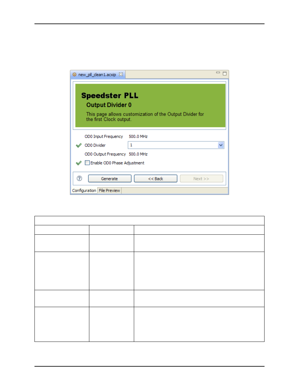
Output Divider [0,1,2,3] Pages
The Output Divider pages contain configuration information relating to the output divider (OD) of one of
the PLLs clock output signals. Since there are one-to-four PLL output signals per PLL, there are also up to
four of these pages. Because the PLL and OD logic may be bypassed on a per-output basis (as configured
on the
), this page may sometimes be hidden, even if the related clock output is
enabled.
Figure 3.6: IP Advanced PLL Editor Output Divider 0 Page
PLL Editor Output Divider Page Options
Option
Editable
Description
OD[0-3] Input
Frequency
The calculated frequency of the input signal as it enters
this OD logic block.
OD[0-3] Divider
Y
The factor by which the signal entering the OD should be
divided before it exits the OD. As this increases, the OD
output frequency decreases. (Unless this OD is in the
external feedback path, in which case increasing this
value does not affect the OD output frequency, but
increases the VCO output frequency.)
OD[0-3] Output
Frequency
The calculated frequency of the output signal as it exits
this OD logic block.
Enable OD[0-3] Phase
Adjustment
Y
Enabling this will allow this OD to perform phase
adjustments on the OD output signal. When enabled, this
activates the related
OD [0,1,2,3] Phase Adjustment Pages
When disabled, the phase adjustment configuration
options remain hidden.
UG001 Rev. 5.0 - 5th December 2012
14