Terminations, Recommended configuration of plated through holes – Northern Connectors Harting DIN 41 612 Connectors User Manual
Page 31
00
.
25
M 29:1
M 58:1
M 58:1
II
I
I
II
M 29:1
M 58:1
M 58:1
II
I
I
II
M 29:1
M 58:1
M 58:1
II
I
I
II
Gen
er
al
in
fo
rma
tio
n
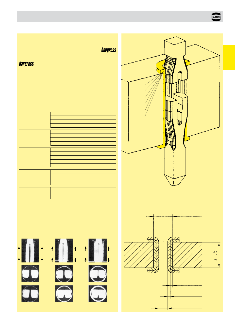
Sketch:
press-in zone
in plated through hole
pcb holes
for press-in
process in acc.
to EN 60 352-5
Sn (HAL)
chem. Sn
Au
Ag
pure Cu
Pd
Recommended configuration of plated
through holes
Due to the high deformation resistance and resilience of
contacts, they can be easily and repeatedly removed in case of
repairs without impairment to their functioning.
is extremely versatile and offers a reliable electrical
contact, therefore it is especially well suited for applications with
these surfaces.
Please contact us for detailed test reports.
In addition to the hot-air-level (HAL) other pcb
surfaces are
getting more important. Due to their different properties, such as
mechanical strength and coefficient of friction we recommend the
following configuration of pcb through holes.
Tin-lead plated
Hole-Ø 1.15
±0.025
mm
PCB
Cu
min. 25 µm
(HAL)
Sn
max. 15 µm
acc. EN 60 352-5
Plated hole-Ø
0.94-1.09 mm
Chemical
Hole-Ø 1.15
±0.025
mm
tin-plated PCB
Cu
min. 25 µm
Sn
min. 0.8 µm
Plated hole-Ø
1.00-1.10 mm
Au / Ni plated PCB
Hole-Ø 1.15
±0.025
mm
Cu
min. 25 µm
Ni
3-7 µm
Au
0.05-0.12 µm
Plated hole-Ø
1.00-1.10 mm
Silver plated PCB
Hole-Ø 1.15
±0.025
mm
Cu
min. 25 µm
Ag
0.1-0.3 µm
Plated hole-Ø
1.00-1.10 mm
OSP
Hole-Ø 1.15
±0.025
mm
copper plated PCB
Cu
min. 25 µm
Plated hole-Ø
1.00-1.10 mm
PCB board thickness: ≥ 1.6 mm
Hole-Ø
Cu
e. g. Sn
Plated hole-Ø
Terminations
Cross section of a pcb 2.4 mm thick with various hole diameters
Diameter
plated through hole
1.09 mm
(max.)
Diameter
plated through hole
0.99-1.00 mm
(nominal)
Diameter
plated through hole
0.92-0.94 mm
(min.)