Wiring of the standard device – Lenze EVS9332xS User Manual
Page 159
Wiring of the standard device
Wiring of digital frequency input / digital frequency output
5.11
l
5.11−2
EDSVS9332S EN 6.0−07/2013
B
Enable (EN)
Lamp
control (LC)
GND
Z
1
2
3
4
5
6
7
8
9
1
2
3
4
5
6
7
8
9
A
X9
X10
< 50 m
A
B
Z
A
A
B
Z
B
Z
9300VEC019
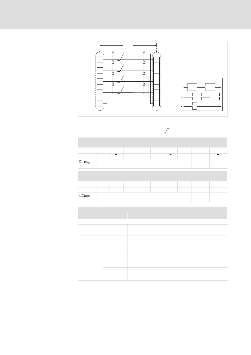
Fig. 5.11−1
Connection of digital frequency input (X9) / digital frequency output (X10)
X9
Slave drive
Signals for CW rotation
X10 Master drive
Cores twisted in pairs
X9 − Digital frequency input
Connector: Pin, 9−pole, Sub−D
Pin
1
2
3
4
5
6
7
8
9
Signal
B
A
A
+5 V
GND
Z
Z
LC
B
0.14 mm
2
(AWG 26)
0.5 mm
2
(AWG 20)
0.14 mm
2
(AWG 26)
0.5 mm
2
(AWG 20)
0.14 mm
2
(AWG 26)
X10 − Digital frequency output
Connector: Socket, 9−pole, Sub−D
Pin
1
2
3
4
5
6
7
8
9
Signal
B
A
A
+5 V
GND
Z
Z
EN
B
0.14 mm
2
(AWG 26)
0.5 mm
2
(AWG 20)
0.14 mm
2
(AWG 26)
0.5 mm
2
(AWG 20)
0.14 mm
2
(AWG 26)
Evaluation of the input signals at X9
Code
Function
C0427 = 0
CW rotation
Track A leads track B by 90 ° (positive value at DFIN−OUT)
CCW rotation
Track A lags track B by 90 ° (negative value at DFIN−OUT)
C0427 = 1
CW rotation
Track A transmits the speed
Track B = LOW (positive value at DFIN−OUT)
CCW rotation
Track A transmits the speed
Track B = HIGH (negative value at DFIN−OUT)
C0427 = 2
CW rotation
Track A transmits the speed and direction of rotation (positive
value at DFIN−OUT)
Track B = LOW
CCW rotation
Track B transmits the speed and direction of rotation (negative
value at DFIN−OUT)
Track A = LOW
Adjustment