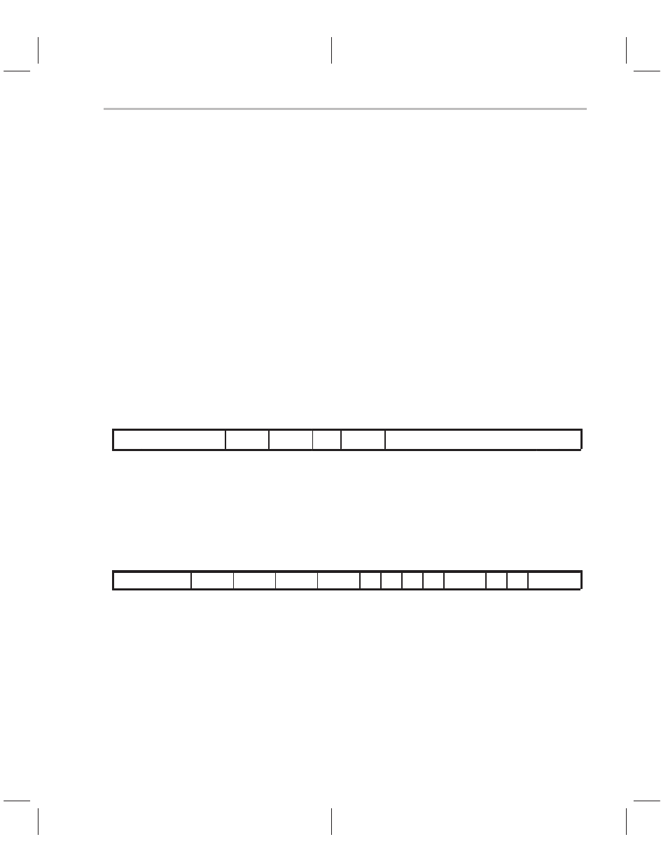
Status registers st0 and st1, 5 status registers st0 and st1, Figure 3–10. status register st0 – Texas Instruments TMS320C2XX User Manual
Page 60: Figure 3–11.status register st1

Status Registers ST0 and ST1
3-15
Central Processing Unit
3.5
Status Registers ST0 and ST1
The ’C2xx has two status registers, ST0 and ST1, which contain status and
control bits. These registers can be stored into and loaded from data memory,
thus allowing the status of the machine to be saved and restored for subrou-
tines.
The LST (load status register) instruction writes to ST0 and ST1, and the SST
(store status register) instruction reads from ST0 and ST1 (with the exception
of the INTM bit, which is not affected by the LST instruction). Many of the indi-
vidual bits of these registers can be set and cleared using the SETC and CLRC
instructions. For example, the sign-extension mode is set with SETC SXM and
cleared with CLRC SXM.
Figure 3–10 and Figure 3–11 show the organization of status registers ST0
and ST1, respectively. Several bits in the status registers are reserved; they
are always read as logic 1s. The other bits are described in alphabetical order
in Table 3–2.
Figure 3–10. Status Register ST0
15
14
13
12
11
10
9
8
7
6
5
4
3
2
1
0
ARP
OV
OVM
ЙЙЙ
ЙЙЙ
1
†
INTM
DP
R/W–x
R/W–0
R/W–x
R/W–1
R/W–x
Note:
R = Read access; W = Write access; value following dash (–) is value after reset (x means value not affected by
reset).
† This reserved bit is always read as 1. Writes have no effect on it.
Figure 3–11.Status Register ST1
15
14
13
12
11
10
9
8
7
6
5
4
3
2
1
0
ARB
CNF
TC
SXM
C
ЙЙ
ЙЙ
1
†
ЙЙ
ЙЙ
1
†
ЙЙЙ
ЙЙЙ
1
†
ЙЙ
ЙЙ
1
†
XF
ЙЙЙ
ЙЙЙ
1
†
ЙЙ
ЙЙ
1
†
PM
R/W–x
R/W–0
R/W–x
R/W–1
R/W–1
R/W–1
R/W–00
Note:
R = Read access; W = Write access; value following dash (–) is value after reset (x means value not affected by
reset).
† These reserved bits are always read as 1s. Writes have no effect on them.
