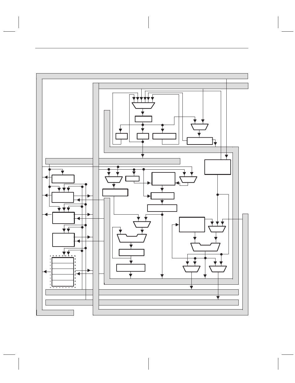
Figure 2–1. overall block diagram of the ’c2xx – Texas Instruments TMS320C2XX User Manual
Page 34

2-2
Figure 2–1. Overall Block Diagram of the ’C2xx
Program
control
PRDB
PRDB
DRDB
DRDB
DWEB
DRAB
DWAB
PAB
DWEB
Stack 8
×
16
MUX
MSTACK
PAR
NPAR
MUX
PC
ROM/flash
SARAM
DARAM
B0
DARAM
B1, B2
ST0
IMR
IFR
GREG
ST1
MUX
Input shifter
Multiplier
16
×
16
TREG
MUX
PREG
Product shifter
Accumulator
Output shifter
Auxiliary
registers
8
×
16
CALU
ARAU
MUX
MUX
MUX
MUX
AR0
DRAB
DWAB
PAB
Note:
The I/O-mapped (peripheral) registers are not part of the core; they are accessed as shown in Figure 2–2 on page 2-4.
Architectural Overview
