Clock generator – Texas Instruments TMS320C2XX User Manual
Page 354

Clock Generator
8-4
8.2
Clock Generator
The high pulse of the master clock output signal (CLKOUT1) signifies the logic
phase of the device (the phase when values are changed), while the low pulse
signifies the latch phase (the phase when values are latched). CLKOUT1 de-
termines much of the device’s operational speed. For example:
-
The timer clock rate is a fraction of the rate of CLKOUT1.
-
Each instruction cycle is equal to one CLKOUT1 period.
-
Each wait state generated by the READY signal or by the on-chip wait-
state generator is equal to one CLKOUT1 period.
You control the rate of CLKOUT1 with the on-chip clock generator. The clock
generator creates an internal CPU clock signal CLKOUT1 whose rate is a frac-
tion or multiple of a source clock signal CLKIN. This generator consists of two
independent components, an oscillator and a phase lock loop (PLL) circuit.
The internal oscillator, in conjunction with an external resonator circuit, allows
you to generate CLKIN internally and create a CLKOUT1 signal that oscillates
at half the frequency of CLKIN. The PLL makes the rate of CLKOUT1 a multiple
of the rate of CLKIN and locks the phase of CLKOUT1 to that of CLKIN.
CLKIN can be generated by the internal oscillator or by an external oscillator:
-
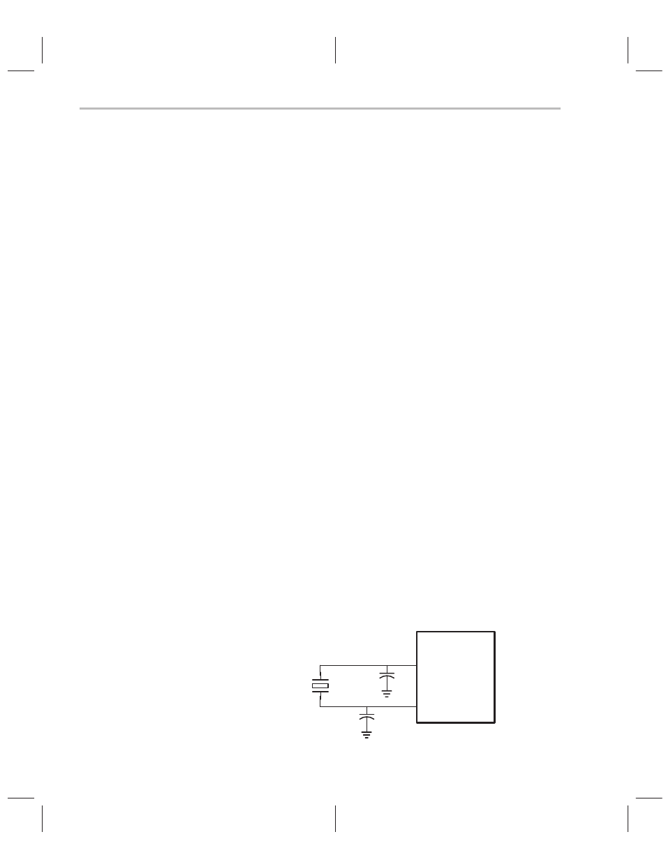
Internal oscillator. The clock source is generated internally by connect-
ing a crystal resonator circuit across the CLKIN/X2 and X1 pins. The crys-
tal should be in either fundamental or overtone operation and parallel res-
onant, with an effective series resistance of 30 ohms and a power dissipa-
tion of 1 mW. It should also be specified at a load capacitance of 20 pF.
Figure 8–1 shows the setup for a fundamental frequency crystal. Over-
tone crystals require an additional tuned-LC circuit.
When the internal oscillator is used, the frequency of CLKOUT1 is half the
oscillating frequency of the crystal. For example, a 40-MHz crystal will pro-
vide a CLKOUT1 rate of 20 MHz, providing 20 MIPS of processing power.
Figure 8–1. Using the Internal Oscillator
’C2xx
X1
CLKIN/X2
Crystal
C
1
C
1
