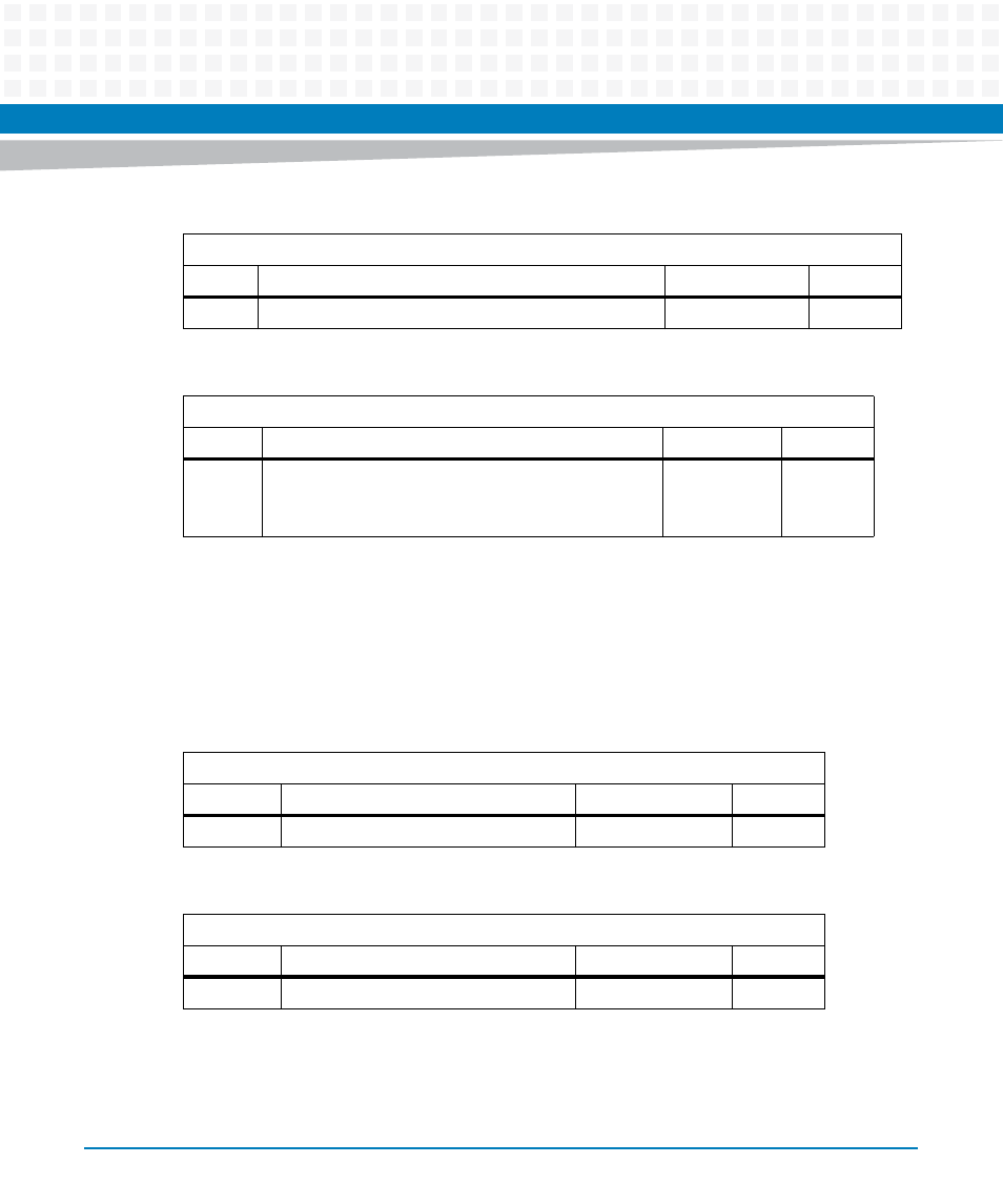
Table 6-77, Telecom ch1_clk1a clock period msb register, Table 6-78 – Artesyn ATCA-7365 Installation and Use (November 2014) User Manual
Page 224: Telecom ch1_clk1a clock period lsb register, Table 6-76, Telecom backplane clocking latch register, Maps and registers

Maps and Registers
ATCA-7365 Installation and Use (6806800K65N)
224
The Clock period of CH1_CLK1A is measured periodically. The result of the measurement
(number of LPC clock cycles) is latched with a write access to the Telecom Backplane Clocking
Latch Register. The 16 bit value is stored in the registers Telecom CH1_CLK1A clock period MSB
Register and Telecom CH1_CLK1A clock period LSB Register. When the clock is static or the
period is higher than a 16 bit value the result is always 0xFFFF.
7:2
Reserved 0
r
Table 6-76 Telecom Backplane Clocking Latch Register
Address Offset: 0x67
Bit
Description
Default
Access
7:0
Latch clock period measurements for CH1_CLK1A and
CH1_CLK1B.
Write data is discarded.
-
LPC: w
Table 6-77 Telecom CH1_CLK1A clock period MSB Register
Address Offset: 0x61
Bit
Description
Default
Access
7:0
MSB of CH1_CLK1A clock period
PWR_GOOD: 0xFF
LPC: r
Table 6-78 Telecom CH1_CLK1A clock period LSB Register
Address Offset: 0x60
Bit
Description
Default
Access
7:0
LSB of CH1_CLK1A clock period
PWR_GOOD: 0xFF
LPC: r
Table 6-75 Telecom Backplane Clocking Status Register
Address Offset: 0x66
Bit
Description
Default
Access
