3 super io configuration registers, Table 6-11, Global configuration register summary – Artesyn ATCA-7365 Installation and Use (November 2014) User Manual
Page 173: Maps and registers
Maps and Registers
ATCA-7365 Installation and Use (6806800K65N)
173
The desired configuration registers are accessed in two steps:
1. Write the index of the Logical Device Number Configuration Register (that is, 07) to the
INDEX PORT and then write the number of the desired logical device to the DATA PORT.
2. Write the address of the desired configuration register within the logical device to the
INDEX PORT and then write or read the configuration register through the DATA PORT.
6.3.3.3
Super IO Configuration Registers
Address locations that are not listed are considered reserved register locations. Reads to
reserved registers may return non-zero values. Writes to reserved locations may cause system
failure.
6.3.3.3.1 Global Control Configuration Registers
The Super IO Global Registers lie in the address range 0x00-0x2F. All eight bits of the ADDRESS
Port are used for register selection. All unimplemented registers and bits ignore writes and
return zero when read. The INDEX PORT is used to select a configuration register in the chip.
The DATA PORT is then used to access the selected register. These registers are accessible only
in the Configuration Mode.
If accessing the Global Configuration Registers, Step 1 is not required. The Super IO returns
to the RUN State.
Only two states are defined (Run and Configuration). In the Run State the Super IO is always
ready to enter the Configuration State.
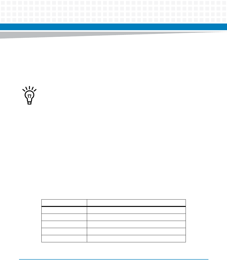
Table 6-11 Global Configuration Register Summary
Index Address
Description
0x07
Super IO Logical Device Number
0x20
Super IO Device ID
0x21
Super IO Device Revision
0x28
Super IO LPC Control
0x29
Super IO SERIRQ and Pre-divide Control