Table 6-37, Scratch register (scr)), Maps and registers – Artesyn ATCA-7365 Installation and Use (November 2014) User Manual
Page 194: 10 scratch register (scr)
Maps and Registers
ATCA-7365 Installation and Use (6806800K65N)
194
6.3.4.2.10 Scratch Register (SCR)
This 8-bit read/write register has no effect on the UART. It is intended as a scratchpad register
for use by the programmer.
4
Complement of the clear-to-send (CTS#) input
When the Asynchronous Communications Element (ACE) is
in diagnostic
test mode (LOOP [MCR4] = 1), this bit is equal to the MCR bit
1 (RTS#).
Ext.
LPC: r
5
Complement of the data set ready (DSR#) input
When the ACE is in the diagnostic test mode (LOOP [MCR4]
= 1), this bit is
equal to the MCR bit 0 (DTR#).
Ext.
LPC: r
6
Complement of the ring indicator (RI#) input
When the ACE is in the diagnostic test mode (LOOP [MCR4]
= 1), this bit is
equal to the MCR bit 2 (OUT1#). Not supported.
Ext.
LPC: r
7
Complement of the data carrier detect (DCD#) input
When the ACE is in the diagnostic test mode (LOOP [MCR4]
= 1), this bit is
equal to the MCR bit 3 (OUT2#). Not supported.
Ext.
LPC: r
Table 6-36 Modem Status Register (MSR) (continued)
LPC IO Address: Base + 6
Bit
Description
Default
Access
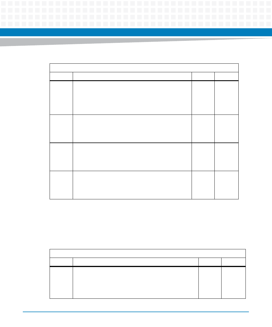
Table 6-37 Scratch Register (SCR))
LPC IO Address: Base + 7
Bit
Description
Default
Access
7:0
Scratch Register (SCR)
The scratch register is an 8 bit register that is intended for the
programmer's use as a scratch pad in the sense that it
temporarily holds the programmer's data without affecting any
other ACE operation.
Undef.
LPC: r/w