Functional description, 1 block diagram, Figure 5-1 – Artesyn ATCA-7365 Installation and Use (November 2014) User Manual
Page 153: Block diagram, Chapter 5
Chapter 5
ATCA-7365 Installation and Use (6806800K65N)
153
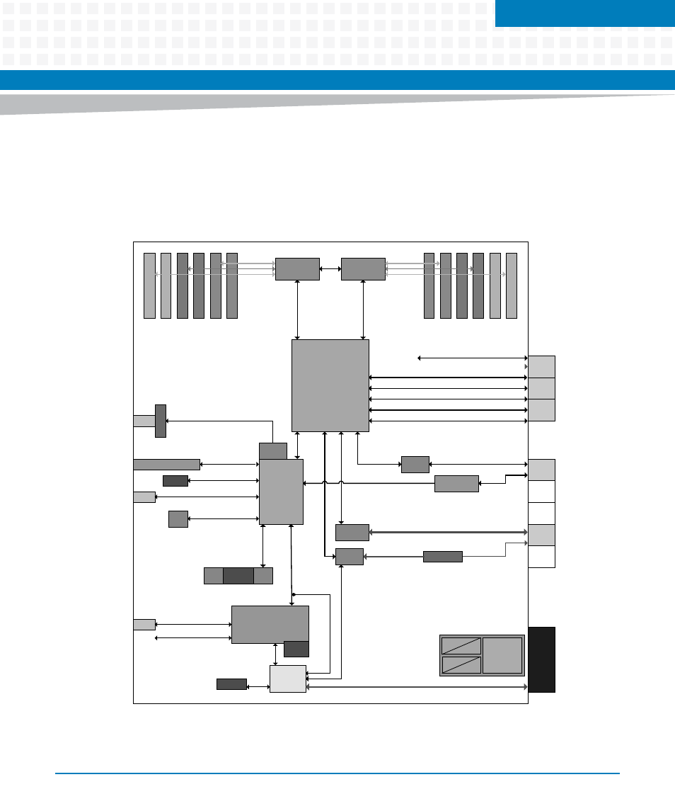
Functional Description
5.1
Block Diagram
The block diagram shows how the devices work together and the data paths are used.
Figure 5-1
Block Diagram
Xeon L5638
Xeon L5638
Intel 5520 Chipset
DDR3
DDR3
QPI
QPI
QPI
6 x DDR3 socket
6 x DDR3 socket
P30
P31
P32
USB2.0
ICH10 Port8
COM_RTM,RST
PCIe x4
PCIe x4
PCIe x4
PCIe x4
PCIe x4
Zone 3
X
F
M
R
10/100/1000Base-T
ICH10
PHY
82567
PMEM/SATA Module
SATA
4GB
SSD
ESI
PCI/SATA
SATA
USB2.0
ICH10
Port 0+2
USB2.0
ICH10 Port 6
SPI
Debug
Socket
Rec.
SPI
SPI
FPGA
COM
COM_RTM
Port80
LED
IPMC
RS232
COM_IPMC
KCS
LPC
82599
(Niantic)
P20
P21
P22
P23
P24
CLK-
INTERRUPT
82572
82576
Kawela
1000Base-BX
SMB: Serial over LAN Pass Through
XF
2x 10GBase-BX4
2x 1000Base-BX
2x 10/100/1000Base-T
Zone 1
IPMB-A/B
3.3V
-48V
FUSING.
EMI,
INRUSH,
5 ms holdup
12V
-48V
5x UC
ATCA3.1 Option1,9
Fabrif IF
ATCA3.0 Base IF
PCIe
x8
PCIe x4
Zone 2