Ocean Optics NanoCalc User Manual
Page 76
Ocean Optics Germany GmbH Thin Film Metrology
75
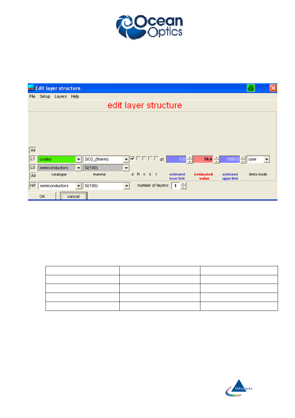
Example I:
Measure SiO
2
on a Si-Wafer
Go to menu Edit layer structure.
Settings:
L1 (layer1)
oxides SiO
2
_(therm)
bulk (substrate) semiconductors Si
ref (reference) semiconductors
Si
user limits
0 nm - 1050 nm
estimated thickness
50 nm
Go to menu Screen > Frequency limits and adjust the plot limits and the extraction range to:
System
max. plot limits [nm]
max. extraction range [nm]
VIS
400 – 850
450 – 800
XR
250 – 1050
300 – 1000
DUV
190 – 1100
220 – 1050
NIR
900 – 1700
950 – 1650
For thin materials choose a bigger range, for thicker materials (NIR) choose a smaller range and set the
smoothing factor 1.
See also other documents in the category Ocean Optics Equipment:
- Apex 785 Raman (1 page)
- STS-UV (2 pages)
- TR2 Engineering Note (4 pages)
- SAD500 Communications and Control (19 pages)
- Red Tide USB650 Install (26 pages)
- Fiber Optic Termination Kit (6 pages)
- Transmissive pH Probe (10 pages)
- Remora (42 pages)
- PlasCalc (59 pages)
- Correcting Device Driver Issues (8 pages)
- ecoVis Krypton Light Source (16 pages)
- LPC-500CM (28 pages)
- HPX-2000 (24 pages)
- ADC1000-USB (27 pages)
- Torus Operating Instructions (30 pages)
- ADC2000-PCI (13 pages)
- Sensors for Real-Time Analysis (2 pages)
- IDRaman reader (2 pages)
- DH-2000-CAL (30 pages)
- QE65 Pro (32 pages)
- Collimating Lenses (2 pages)
- D1000 (2 pages)
- IDRaman mini (2 pages)
- HR2000CG-UV-NIR (42 pages)
- Cool Red (1 page)
- HL-2000 (20 pages)
- XE-1 Xenon (6 pages)
- USB-ADP Serial Adapters (3 pages)
- CHEM2000 (36 pages)
- Deuterium-Halogen Calibration Light Source (19 pages)
- NeoFox Engineering Note (30 pages)
- QE Pro (2 pages)
- OOIBase32 (140 pages)
- AR-1 Argon (6 pages)
- pH Sensor Patches, Probes and Cuvettes (36 pages)
- SpecLine Offline Spectroscopy (60 pages)
- HL-2000-HP-232 (26 pages)
- External Triggering Options Instructions for Spectrometers with Firmware Version 3.0 and Above (16 pages)
- Breakout Box (10 pages)
- USB-ISS-UV_VIS (4 pages)
- ISS-UV_VIS (6 pages)
- OOIColor (14 pages)
- LS-1 Series (12 pages)
- Apex Install (24 pages)
- DH-2000 (34 pages)