4 adcl – adc data register, 5 didr0 – digital input disable register 0, Adcl – Rainbow Electronics ATtiny10 User Manual
Page 95
95
8127B–AVR–08/09
ATtiny4/5/9/10
trigger signal. If ADEN in ADCSRA is set, this will start a conversion. Switching to Free Running
mode (ADTS[2:0]=0) will not cause a trigger event, even if the ADC Interrupt Flag is set
.
13.12.4
ADCL
–
ADC Data Register
When an ADC conversion is complete, the result is found in the ADC register.
• Bits 7:0 – ADC7:0: ADC Conversion Result
These bits represent the result from the conversion.
13.12.5
DIDR0
–
Digital Input Disable Register 0
• Bits 7:4 – Res: Reserved Bit
These bits are reserved and will always read zero.
• Bits 3:0 – ADC3D..ADC0D: ADC3..0 Digital Input Disable
When this bit is written logic one, the digital input buffer on the corresponding ADC pin is dis-
abled. The corresponding PIN register bit will always read as zero when this bit is set. When an
analog signal is applied to the ADC3..0 pin and the digital input from this pin is not needed, this
bit should be written logic one to reduce power consumption in the digital input buffer.
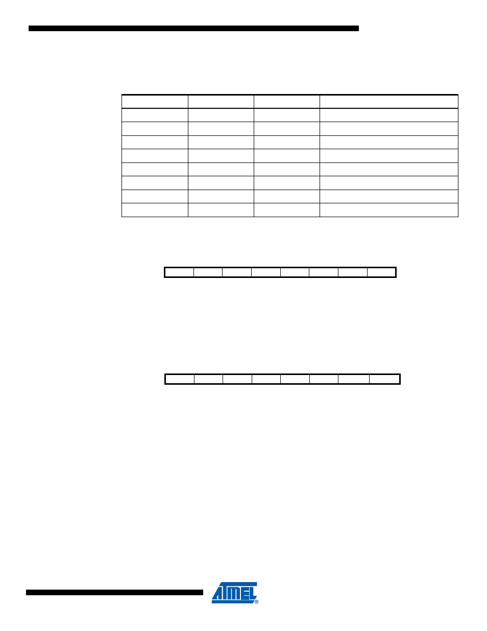
Table 13-4.
ADC Auto Trigger Source Selections
ADTS2
ADTS1
ADTS0
Trigger Source
0
0
0
Free Running mode
0
0
1
Analog Comparator
0
1
0
External Interrupt Flag 0
0
1
1
Timer/Counter 0 Compare Match A
1
0
0
Timer/Counter 0 Overflow
1
0
1
Timer/Counter 0 Compare Match B
1
1
0
Pin Change Interrupt 0 Request
1
1
1
Timer/Counter 0 Capture Event
Bit
7
6
5
4
3
2
1
0
0x19
ADC7
ADC6
ADC5
ADC4
ADC3
ADC2
ADC1
ADC0
ADCL
Read/Write
R
R
R
R
R
R
R
R
Initial Value
0
0
0
0
0
0
0
0
Bit
7
6
5
4
3
2
1
0
0x17
–
–
–
–
ADC3D
ADC2D
ADC1D
ADC0D
DIDR0
Read/Write
R
R
R
R
R/W
R/W
R/W
R/W
Initial Value
0
0
0
0
0
0
0
0