2 tccr0b – timer/counter0 control register b – Rainbow Electronics ATtiny10 User Manual
Page 75
75
8127B–AVR–08/09
ATtiny4/5/9/10
• Bits 1:0 – WGM01:0: Waveform Generation Mode
Combined with WGM03:2 bits of TCCR0B, these bits control the counting sequence of the coun-
ter, the source for maximum (TOP) counter value, and what type of waveform to generate. See
Table 11-5
. Modes of operation supported by the Timer/Counter unit are: Normal mode (coun-
ter), Clear Timer on Compare match (CTC) mode, and three types of Pulse Width Modulation
(PWM) modes. (
“Modes of Operation” on page 62
).
11.11.2
TCCR0B – Timer/Counter0 Control Register B
• Bit 7 – ICNC0: Input Capture Noise Canceler
Setting this bit (to one) activates the Input Capture Noise Canceler. When the noise canceler is
activated, the input from the Input Capture pin (ICP0) is filtered. The filter function requires four
successive equal valued samples of the ICP0 pin for changing its output. The Input Capture is
therefore delayed by four oscillator cycles when the noise canceler is enabled.
• Bit 6 – ICES0: Input Capture Edge Select
This bit selects which edge on the Input Capture pin (ICP0) that is used to trigger a capture
event. When the ICES0 bit is written to zero, a falling (negative) edge is used as trigger, and
when the ICES0 bit is written to one, a rising (positive) edge will trigger the capture.
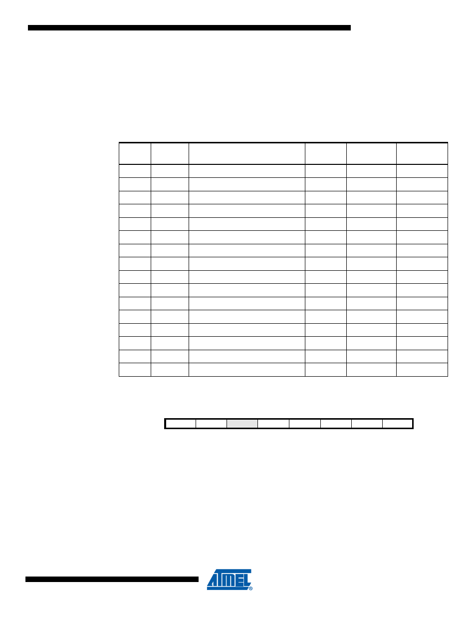
Table 11-5.
Waveform Generation Modes
Mode
WGM
0
3:0
Mode of Operation
TOP
Update of
OCR0
x
at
TOV0 Flag
Set on
0
0000
Normal
0xFFFF
Immediate
MAX
1
0001
PWM, Phase Correct, 8-bit
0x00FF
TOP
BOTTOM
2
0010
PWM, Phase Correct, 9-bit
0x01FF
TOP
BOTTOM
3
0011
PWM, Phase Correct, 10-bit
0x03FF
TOP
BOTTOM
4
0100
CTC (
Clear Timer on Compare
)
OCR0A
Immediate
MAX
5
0101
Fast PWM, 8-bit
0x00FF
TOP
TOP
6
0110
Fast PWM, 9-bit
0x01FF
TOP
TOP
7
0111
Fast PWM, 10-bit
0x03FF
TOP
TOP
8
1000
PWM, Phase & Freq. Correct
ICR0
BOTTOM
BOTTOM
9
1001
PWM, Phase & Freq. Correct
OCR0A
BOTTOM
BOTTOM
10
1010
PWM, Phase Correct
ICR0
TOP
BOTTOM
11
1011
PWM, Phase Correct
OCR0A
TOP
BOTTOM
12
1100
CTC (
Clear Timer on Compare
)
ICR0
Immediate
MAX
13
1101
(Reserved)
–
–
–
14
1110
Fast PWM
ICR0
TOP
TOP
15
1111
Fast PWM
OCR0A
TOP
TOP
Bit
7
6
5
4
3
2
1
0
0x2D
ICNC0
ICES0
–
WGM03
WGM02
CS02
CS01
CS00
TCCR0B
Read/Write
R/W
R/W
R
R/W
R/W
R/W
R/W
R/W
Initial Value
0
0
0
0
0
0
0
0