1 data memory access times, 3 i/o memory – Rainbow Electronics ATtiny10 User Manual
Page 15
15
8127B–AVR–08/09
ATtiny4/5/9/10
Figure 5-1.
Data Memory Map (Byte Addressing)
5.2.1
Data Memory Access Times
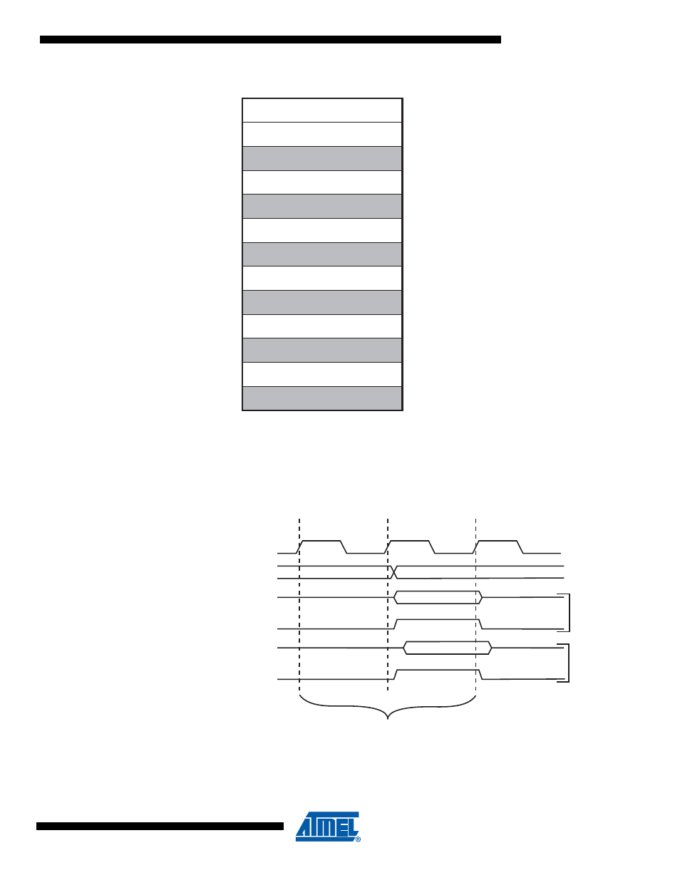
This section describes the general access timing concepts for internal memory access. The
internal data SRAM access is performed in two clk
CPU
cycles as described in
Figure 5-2
.
Figure 5-2.
On-chip Data SRAM Access Cycles
5.3
I/O Memory
The I/O space definition of the ATtiny4/5/9/10 is shown in
“Register Summary” on page 149
.
0x0000 ... 0x003F
0x0040 ... 0x005F
0x0060 ... 0x3EFF
0x3F00 ... 0x3F01
0x3F02 ... 0x3F3F
0x3F40 ... 0x3F41
0x3F42 ... 0x3F7F
0x3F80 ... 0x3F81
0x3F82 ... 0x3FBF
0x3FC0 ... 0x3FC3
0x3FC4 ... 0x3FFF
0x4000 ... 0x41FF/0x43FF
0x4400 ... 0xFFFF
I/O SPACE
SRAM DATA MEMORY
(reserved)
NVM LOCK BITS
(reserved)
CONFIGURATION BITS
(reserved)
CALIBRATION BITS
(reserved)
DEVICE ID BITS
(reserved)
FLASH PROGRAM MEMORY
(reserved)
clk
WR
RD
Data
Data
Address
Address valid
T1
T2
T3
Compute Address
Read
Wr
ite
CPU
Memory Access Instruction
Next Instruction
- MAX5151 (16 pages)
- MAXQ3108 (64 pages)
- MAX5661 (39 pages)
- MAX6691 (7 pages)
- MAX5362 (12 pages)
- ADC10158 (26 pages)
- MAX8922L (14 pages)
- MAX8596Z (8 pages)
- MAX7491 (18 pages)
- MAX15040 (15 pages)
- MAX5177 (16 pages)
- ADC08138 (22 pages)
- MAX5961 (42 pages)
- T89C51RD2 (86 pages)
- MAX16055 (9 pages)
- MAX6659 (17 pages)
- ADC0820 (20 pages)
- MAX6678 (19 pages)
- MAX8884Z (15 pages)
- MAX16915 (9 pages)
- MAX8620 (18 pages)
- MAX5144 (12 pages)
- MAX6670 (8 pages)
- MAX8760 (39 pages)
- W78C32C (14 pages)
- MX7533 (8 pages)
- MAX8727 (13 pages)
- MAX9053 (15 pages)
- W78C54 (16 pages)
- MAX8614B (15 pages)
- W90N740 (219 pages)
- MAX6626 (13 pages)
- ADC10738 (30 pages)
- MAX17000 (31 pages)
- MAX5051 (21 pages)
- MAXQ1004 (18 pages)
- MAX6871 (51 pages)
- MX7847 (12 pages)
- MAX6608 (6 pages)
- MAX17083 (15 pages)
- MAX6641 (17 pages)
- MAX5251 (16 pages)
- MAX6338 (8 pages)
- MAX6690 (16 pages)
- MAX8668 (18 pages)