12 register description, 1 admux – adc multiplexer selection register, 2 adcsra – adc control and status register a – Rainbow Electronics ATtiny10 User Manual
Page 93: Admux – adc multiplexer
93
8127B–AVR–08/09
ATtiny4/5/9/10
13.12 Register Description
13.12.1
ADMUX
–
ADC Multiplexer Selection Register
• Bits 7:2 – Res: Reserved Bits
These bits are reserved and will always read zero.
• Bits 1:0 – MUX1:0: Analog Channel Selection Bits
The value of these bits selects which combination of analog inputs are connected to the ADC.
See
Table 13-2
for details.
If these bits are changed during a conversion, the change will not go
in effect until the conversion is complete (ADIF in ADCSRA is set).
13.12.2
ADCSRA
–
ADC Control and Status Register A
• Bit 7 – ADEN: ADC Enable
Writing this bit to one enables the ADC. By writing it to zero, the ADC is turned off. Turning the
ADC off while a conversion is in progress, will terminate this conversion.
• Bit 6 – ADSC: ADC Start Conversion
In Single Conversion mode, write this bit to one to start each conversion. In Free Running mode,
write this bit to one to start the first conversion. The first conversion after ADSC has been written
after the ADC has been enabled, or if ADSC is written at the same time as the ADC is enabled,
will take 25 ADC clock cycles instead of the normal 13. This first conversion performs initializa-
tion of the ADC.
ADSC will read as one as long as a conversion is in progress. When the conversion is complete,
it returns to zero. Writing zero to this bit has no effect.
• Bit 5 – ADATE: ADC Auto Trigger Enable
When this bit is written to one, Auto Triggering of the ADC is enabled. The ADC will start a con-
version on a positive edge of the selected trigger signal. The trigger source is selected by setting
the ADC Trigger Select bits, ADTS in ADCSRB.
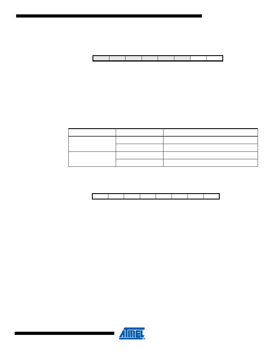
Bit
7
6
5
4
3
2
1
0
0x1B
–
–
–
–
–
–
MUX1
MUX0
ADMUX
Read/Write
R
R
R
R
R
R
R/W
R/W
Initial Value
0
0
0
0
0
0
0
0
Table 13-2.
Input Channel Selections
MUX1
MUX0
Single Ended Input
0
0
ADC0 (PB0)
1
ADC1 (PB1)
1
0
ADC2 (PB2)
1
ADC3 (PB3)
Bit
7
6
5
4
3
2
1
0
0x1D
ADEN
ADSC
ADATE
ADIF
ADIE
ADPS2
ADPS1
ADPS0
ADCSRA
Read/Write
R/W
R/W
R/W
R/W
R/W
R/W
R/W
R/W
Initial Value
0
0
0
0
0
0
0
0