10 accessing 16-bit registers, Accessing 16-bit registers” on – Rainbow Electronics ATtiny10 User Manual
Page 71
71
8127B–AVR–08/09
ATtiny4/5/9/10
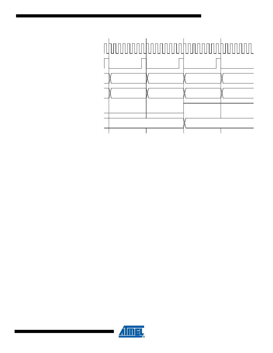
Figure 11-15. Timer/Counter Timing Diagram, with Prescaler (f
clk_I/O
/8)
11.10 Accessing 16-bit Registers
The TCNT0, OCR0A/B, and ICR0 are 16-bit registers that can be accessed by the AVR CPU via
the 8-bit data bus. The 16-bit register must be byte accessed using two read or write operations.
Each 16-bit timer has a single 8-bit register for temporary storing of the high byte of the 16-bit
access. The same temporary register is shared between all 16-bit registers within each 16-bit
timer. Accessing the low byte triggers the 16-bit read or write operation. When the low byte of a
16-bit register is written by the CPU, the high byte stored in the temporary register, and the low
byte written are both copied into the 16-bit register in the same clock cycle. When the low byte of
a 16-bit register is read by the CPU, the high byte of the 16-bit register is copied into the tempo-
rary register in the same clock cycle as the low byte is read.
Not all 16-bit accesses uses the temporary register for the high byte. Reading the OCR0A/B 16-
bit registers does not involve using the temporary register.
To do a 16-bit write, the high byte must be written before the low byte. For a 16-bit read, the low
byte must be read before the high byte.
The following code example shows how to access the 16-bit timer registers assuming that no
interrupts updates the temporary register. The same principle can be used directly for accessing
the OCR0A/B and ICR0 Registers.
TOVn
(FPWM)
and ICF n
(if used
as TOP)
OCRnx
(Update at TOP)
TCNTn
(CTC and FPWM)
TCNTn
(PC and PFC PWM)
TOP - 1
TOP
TOP - 1
TOP - 2
Old OCRnx Value
New OCRnx Value
TOP - 1
TOP
BOTTOM
BOTTOM + 1
clk
I/O
clk
Tn
(clk
I/O
/8)