1 reusing the temporary high byte register, 11 register description, 1 tccr0a – timer/counter0 control register a – Rainbow Electronics ATtiny10 User Manual
Page 73
73
8127B–AVR–08/09
ATtiny4/5/9/10
Note:
See
The code example requires that the r17:r16 register pair contains the value to be written to
TCNT0.
11.10.1
Reusing the Temporary High Byte Register
If writing to more than one 16-bit register where the high byte is the same for all registers written,
then the high byte only needs to be written once. However, note that the same rule of atomic
operation described previously also applies in this case.
11.11 Register Description
11.11.1
TCCR0A – Timer/Counter0 Control Register A
• Bits 7:6 – COM0A1:0: Compare Output Mode for Channel A
• Bits 5:4 – COM0B1:0: Compare Output Mode for Channel B
The COM0A1:0 and COM0B1:0 control the behaviour of Output Compare pins OC0A and
OC0B, respectively. If one or both COM0A1:0 bits are written to one, the OC0A output overrides
the normal port functionality of the I/O pin it is connected to. Similarly, if one or both COM0B1:0
bit are written to one, the OC0B output overrides the normal port functionality of the I/O pin it is
connected to.
Note, however, that the Data Direction Register (DDR) bit corresponding to the OC0A or OC0B
pin must be set in order to enable the output driver.
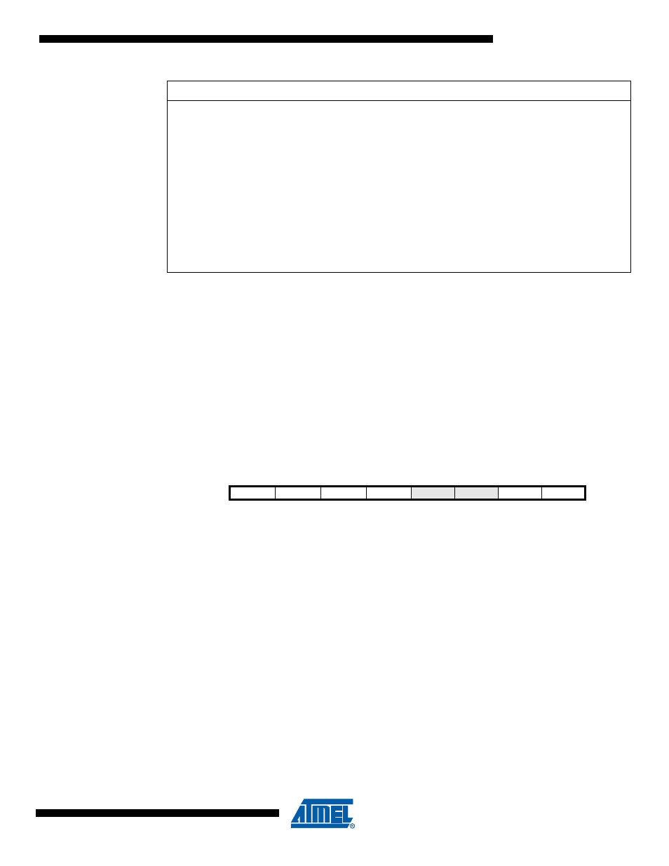
Assembly Code Example
TIM16_WriteTCNT
0:
; Save global interrupt flag
in
r18,SREG
; Disable interrupts
cli
; Set TCNT
0 to r17:r16
out
TCNT
0H,r17
out
TCNT
0L,r16
; Restore global interrupt flag
out
SREG,r18
ret
Bit
7
6
5
4
3
2
1
0
0x2E
COM0A1
COM0A0
COM0B1
COM0B0
–
–
WGM01
WGM00
TCCR0A
Read/Write
R/W
R/W
R/W
R/W
R
R
R/W
R/W
Initial Value
0
0
0
0
0
0
0
0