8 analog input circuitry – Rainbow Electronics ATtiny10 User Manual
Page 89
89
8127B–AVR–08/09
ATtiny4/5/9/10
• Make sure that the ADC is enabled and is not busy converting. Single Conversion mode must
be selected and the ADC conversion complete interrupt must be enabled.
• Enter ADC Noise Reduction mode (or Idle mode). The ADC will start a conversion once the
CPU has been halted.
• If no other interrupts occur before the ADC conversion completes, the ADC interrupt will wake
up the CPU and execute the ADC Conversion Complete interrupt routine. If another interrupt
wakes up the CPU before the ADC conversion is complete, that interrupt will be executed,
and an ADC Conversion Complete interrupt request will be generated when the ADC
conversion completes. The CPU will remain in active mode until a new sleep command is
executed.
Note that the ADC will not be automatically turned off when entering other sleep modes than Idle
mode and ADC Noise Reduction mode. The user is advised to write zero to ADEN before enter-
ing such sleep modes to avoid excessive power consumption.
13.8
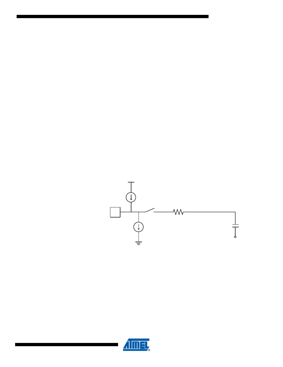
Analog Input Circuitry
The analog input circuitry for single ended channels is illustrated in
Figure 13-8
An analog
source applied to ADCn is subjected to the pin capacitance and input leakage of that pin, regard-
less of whether that channel is selected as input for the ADC. When the channel is selected, the
source must drive the S/H (sample and hold) capacitor through the series resistance (combined
resistance in the input path).
Figure 13-8. Analog Input Circuitry
The capacitor in
Figure 13-8
depicts the total capacitance, including the sample/hold capacitor
and any stray or parasitic capacitance inside the device. The value given is worst case.
The ADC is optimized for analog signals with an output impedance of approximately 10 k
Ω
, or
less. With such sources, the sampling time will be negligible. If a source with higher impedance
is used, the sampling time will depend on how long time the source needs to charge the S/H
capacitor. This can vary widely. The user is recommended to only use low impedance sources
with slowly varying signals, since this minimizes the required charge transfer to the S/H
capacitor.
Signal components higher than the Nyquist frequency (f
ADC
/2) should not be present to avoid
distortion from unpredictable signal convolution. The user is advised to remove high frequency
components with a low-pass filter before applying the signals as inputs to the ADC.
ADCn
I
IH
1..100 k
ohm
C
S/H
= 14 pF
V
CC
/2
I
IL