3 register description, 1 eicra – external interrupt control register a, Figure 9-1. timing of pin change interrupts – Rainbow Electronics ATtiny10 User Manual
Page 37
37
8127B–AVR–08/09
ATtiny4/5/9/10
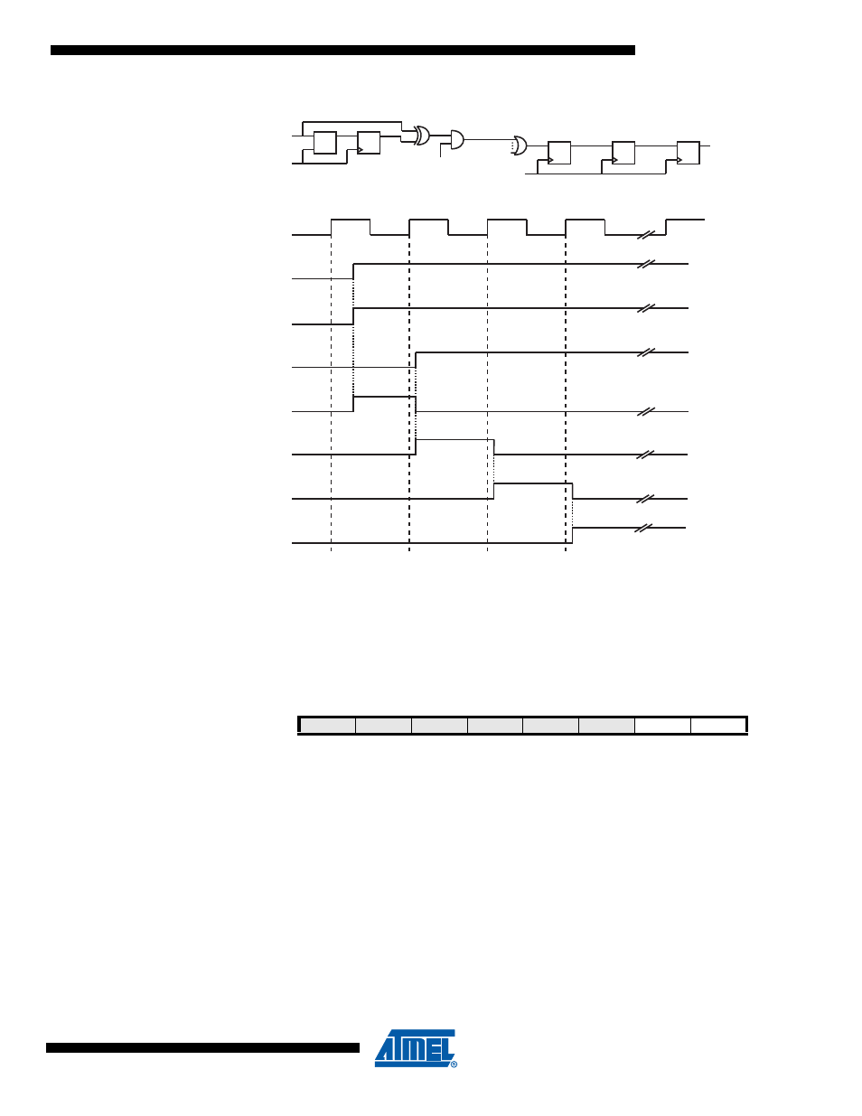
Figure 9-1.
Timing of pin change interrupts
9.3
Register Description
9.3.1
EICRA – External Interrupt Control Register A
The External Interrupt Control Register A contains control bits for interrupt sense control.
• Bits 7:2 – Res: Reserved Bits
These bits are reserved and will always read zero.
• Bits 1:0 – ISC01, ISC00: Interrupt Sense Control 0 Bit 1 and Bit 0
The External Interrupt 0 is activated by the external pin INT0 if the SREG I-flag and the corre-
sponding interrupt mask are set. The level and edges on the external INT0 pin that activate the
interrupt are defined in
Table 9-2
. The value on the INT0 pin is sampled before detecting edges.
If edge or toggle interrupt is selected, pulses that last longer than one clock period will generate
an interrupt. Shorter pulses are not guaranteed to generate an interrupt. If low level interrupt is
clk
PCINT(0)
pin_lat
pin_sync
pcint_in_(0)
pcint_syn
pcint_setflag
PCIF
PCINT(0)
pin_sync
pcint_syn
pin_lat
D Q
LE
pcint_setflag
PCIF
clk
clk
PCINT(0) in PCMSK(x)
pcint_in_(0)
0
x
Bit
7
6
5
4
3
2
1
0
0x15
–
–
–
–
–
–
ISC01
ISC00
EICRA
Read/Write
R
R
R
R
R
R
R/W
R/W
Initial Value
0
0
0
0
0
0
0
0