2 reading the flash, 3 programming the flash, 1 chip erase – Rainbow Electronics ATtiny10 User Manual
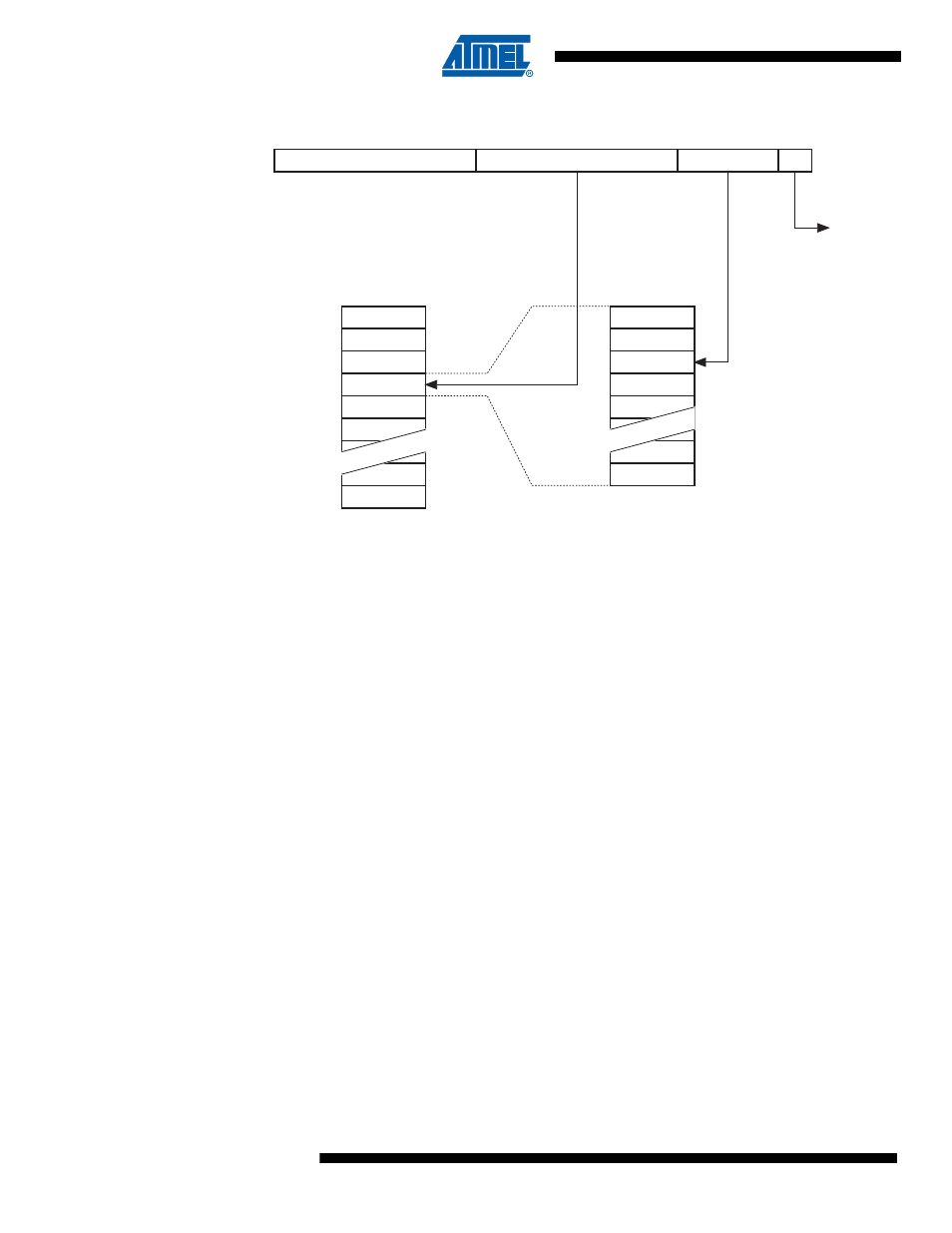
Page 112: Is illustrated in, Figure 15-1
112
8127B–AVR–08/09
ATtiny4/5/9/10
Figure 15-1. Addressing the Flash Memory
15.4.2
Reading the Flash
The Flash can be read from the data memory mapped locations one byte at a time. For read
operations, the least significant bit (bit 0) is used to select the low or high byte in the word
address. If this bit is zero, the low byte is read, and if it is one, the high byte is read.
15.4.3
Programming the Flash
The Flash can be written word-by-word. Before writing a Flash word, the Flash target location
must be erased. Writing to an un-erased Flash word will corrupt its content.
The Flash is word-accessed for writing, and the data space uses byte-addressing to access
Flash that has been mapped to data memory. It is therefore important to write the word in the
correct order to the Flash, namely low bytes before high bytes. First, the low byte is written to the
temporary buffer. Then, writing the high byte latches both the high byte and the low byte into the
Flash word buffer, starting the write operation to Flash.
The Flash erase operations can only performed for the entire Flash sections.
The Flash programming sequence is as follows:
1.
Perform a Flash section erase or perform a Chip erase
2.
Write the Flash section word by word
15.4.3.1
Chip Erase
The Chip Erase command will erase the entire code section of the Flash memory and the NVM
Lock Bits. For security reasons, the NVM Lock Bits are not reset before the code section has
been completely erased. Configuration, Signature and Calibration sections are not changed.
00
PAGE
01
02
SECTIONEND
WORD
00
01
PAGEEND
FLASH
SECTION
FLASH
PAGE
0/1
WADDR
PADDR
1
WADDRMSB
PADDRMSB
16
ADDRESS POINTER
...
...
...
...
...
...
PAGE ADDRESS
WITHIN A FLASH
SECTION
WORD ADDRESS
WITHIN A FLASH
PAGE
LOW/HIGH
BYTE SELECT
WADDRMSB+1