4 reading the pin value, Figure 10-3, Instructions sync latch pinxn r17 – Rainbow Electronics ATtiny10 User Manual
Page 43: System clk
43
8127B–AVR–08/09
ATtiny4/5/9/10
Figure 10-3. Switching Between Input and Output in Break-Before-Make-Mode
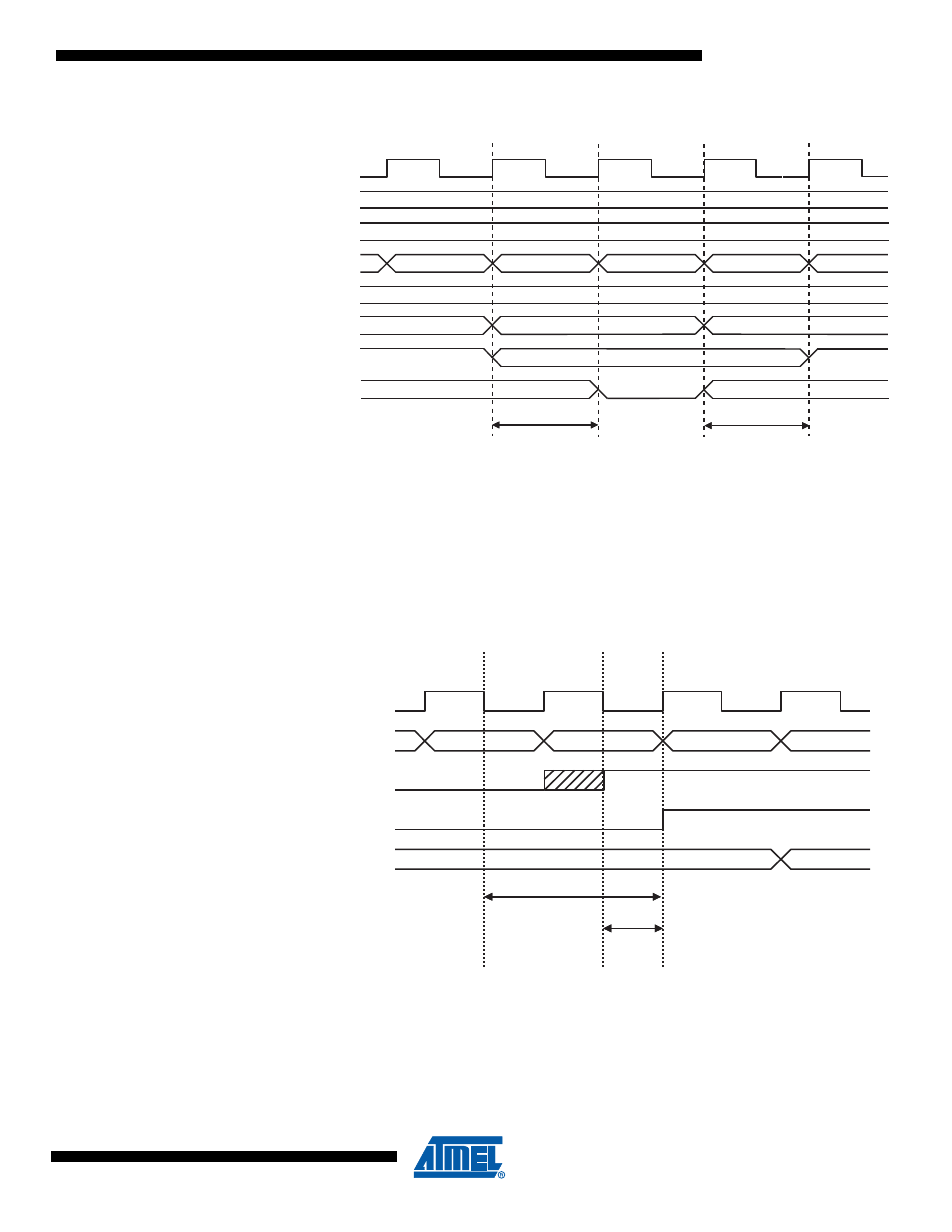
10.2.4
Reading the Pin Value
Independent of the setting of Data Direction bit DDxn, the port pin can be read through the
PINxn Register bit. As shown in
Figure 10-2 on page 41
, the PINxn Register bit and the preced-
ing latch constitute a synchronizer. This is needed to avoid metastability if the physical pin
changes value near the edge of the internal clock, but it also introduces a delay.
Figure 10-4
shows a timing diagram of the synchronization when reading an externally applied pin value.
The maximum and minimum propagation delays are denoted t
pd,max
and t
pd,min
respectively.
Figure 10-4. Synchronization when Reading an Externally Applied Pin value
Consider the clock period starting shortly after the first falling edge of the system clock. The latch
is closed when the clock is low, and goes transparent when the clock is high, as indicated by the
shaded region of the “SYNC LATCH” signal. The signal value is latched when the system clock
goes low. It is clocked into the PINxn Register at the succeeding positive clock edge. As indi-
cated by the two arrows tpd,max and tpd,min, a single signal transition on the pin will be delayed
between ½ and 1½ system clock period depending upon the time of assertion.
out DDRx, r16
nop
0x02
0x01
SYSTEM CLK
INSTRUCTIONS
DDRx
intermediate tri-state cycle
out DDRx, r17
0x55
PORTx
0x01
intermediate tri-state cycle
Px0
Px1
tri-state
tri-state
tri-state
0x01
r17
0x02
r16
XXX
in r17, PINx
0x00
0xFF
INSTRUCTIONS
SYNC LATCH
PINxn
r17
XXX
SYSTEM CLK
t
pd, max
t
pd, min