9 noise canceling techniques, 10 adc accuracy definitions – Rainbow Electronics ATtiny10 User Manual
Page 90
90
8127B–AVR–08/09
ATtiny4/5/9/10
13.9
Noise Canceling Techniques
Digital circuitry inside and outside the device generates EMI which might affect the accuracy of
analog measurements. When conversion accuracy is critical, the noise level can be reduced by
applying the following techniques:
• Keep analog signal paths as short as possible.
• Make sure analog tracks run over the analog ground plane.
• Keep analog tracks well away from high-speed switching digital tracks.
• If any port pin is used as a digital output, it mustn’t switch while a conversion is in progress.
• Place bypass capacitors as close to V
CC
and GND pins as possible.
Where high ADC accuracy is required it is recommended to use ADC Noise Reduction Mode, as
described in
. A good system design with properly placed, external
bypass capacitors does reduce the need for using ADC Noise Reduction Mode
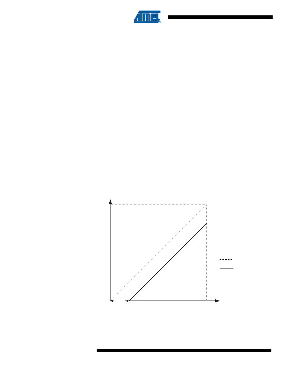
13.10 ADC Accuracy Definitions
An n-bit single-ended ADC converts a voltage linearly between GND and V
REF
in 2
n
steps
(LSBs). The lowest code is read as 0, and the highest code is read as 2
n
-1.
Several parameters describe the deviation from the ideal behavior:
• Offset: The deviation of the first transition (0x00 to 0x01) compared to the ideal transition (at
0.5 LSB). Ideal value: 0 LSB.
Figure 13-9. Offset Error
Output Code
V
REF
Input Voltage
Ideal ADC
Actual ADC
Offset
Error