2 ports as general digital i/o, 1 configuring the pin, Da ta bus – Rainbow Electronics ATtiny10 User Manual
Page 41
41
8127B–AVR–08/09
ATtiny4/5/9/10
10.2
Ports as General Digital I/O
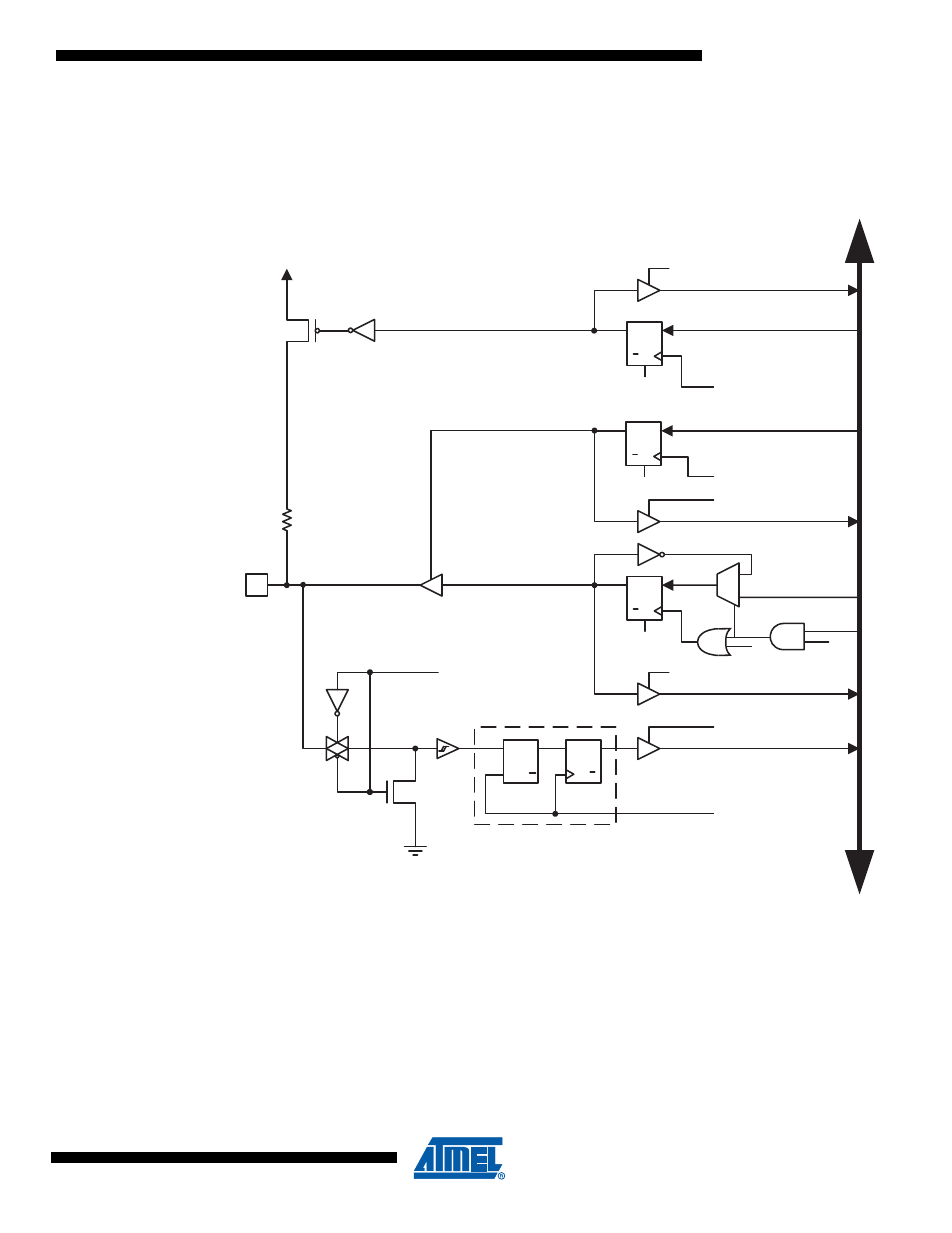
The ports are bi-directional I/O ports with optional internal pull-ups.
Figure 10-2
shows a func-
tional description of one I/O-port pin, here generically called Pxn.
Figure 10-2. General Digital I/O
(1)
Note:
1. WEx, WRx, WPx, WDx, REx, RRx, RPx, and RDx are common to all pins within the same
port. clk
I/O
, and SLEEP are common to all ports.
10.2.1
Configuring the Pin
Each port pin consists of four register bits: DDxn, PORTxn, PUExn, and PINxn. As shown in
“Register Description” on page 50
, the DDxn bits are accessed at the DDRx I/O address, the
PORTxn bits at the PORTx I/O address, the PUExn bits at the PUEx I/O address, and the PINxn
bits at the PINx I/O address.
clk
RPx
RRx
RDx
WDx
WEx
SYNCHRONIZER
WDx:
WRITE DDRx
WRx:
WRITE PORTx
RRx:
READ PORTx REGISTER
RPx:
READ PORTx PIN
clk
I/O
:
I/O CLOCK
RDx:
READ DDRx
WEx:
WRITE PUEx
REx:
READ PUEx
D
L
Q
Q
REx
RESET
RESET
Q
Q
D
Q
Q
D
CLR
PORTxn
Q
Q
D
CLR
DDxn
PINxn
D
A
TA
BUS
SLEEP
SLEEP:
SLEEP CONTROL
Pxn
I/O
WPx
RESET
Q
Q
D
CLR
PUExn
0
1
WRx
WPx:
WRITE PINx REGISTER