Figure 10-6. alternate port functions, Da ta bus – Rainbow Electronics ATtiny10 User Manual
Page 46
46
8127B–AVR–08/09
ATtiny4/5/9/10
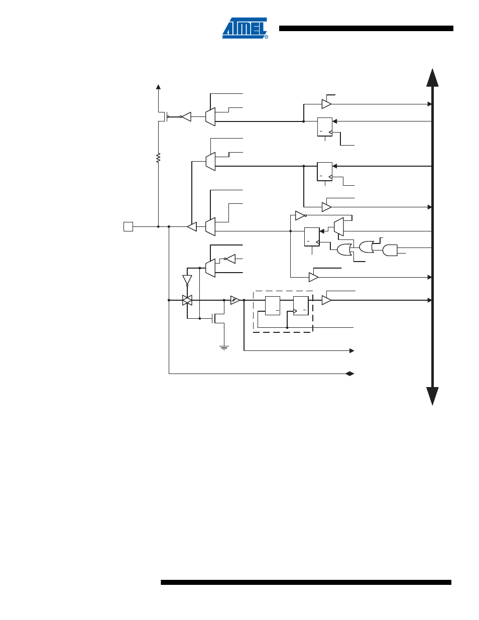
Figure 10-6. Alternate Port Functions
(1)
Note:
1. WEx, WRx, WPx, WDx, REx, RRx, RPx, and RDx are common to all pins within the same
port. clk
I/O
, and SLEEP are common to all ports. All other signals are unique for each pin.
The illustration in the figure above serves as a generic description applicable to all port pins in
the AVR microcontroller family. Some overriding signals may not be present in all port pins.
clk
RPx
RRx
WRx
RDx
WDx
SYNCHRONIZER
WDx:
WRITE DDRx
WRx:
WRITE PORTx
RRx:
READ PORTx REGISTER
RPx:
READ PORTx PIN
REx:
READ PUEx
WEx:
WRITE PUEx
clk
I/O
:
I/O CLOCK
RDx:
READ DDRx
D
L
Q
Q
SET
CLR
0
1
0
1
0
1
DIxn
AIOxn
DIEOExn
PVOVxn
PVOExn
DDOVxn
DDOExn
PUOExn
PUOVxn
PUOExn:
Pxn PULL-UP OVERRIDE ENABLE
PUOVxn:
Pxn PULL-UP OVERRIDE VALUE
DDOExn:
Pxn DATA DIRECTION OVERRIDE ENABLE
DDOVxn:
Pxn DATA DIRECTION OVERRIDE VALUE
PVOExn:
Pxn PORT VALUE OVERRIDE ENABLE
PVOVxn:
Pxn PORT VALUE OVERRIDE VALUE
DIxn:
DIGITAL INPUT PIN n ON PORTx
AIOxn:
ANALOG INPUT/OUTPUT PIN n ON PORTx
RESET
RESET
Q
Q
D
CLR
Q
Q
D
CLR
Q
Q
D
CLR
PINxn
PORTxn
DDxn
D
A
TA
BUS
0
1
DIEOVxn
SLEEP
DIEOExn:
Pxn DIGITAL INPUT-ENABLE OVERRIDE ENABLE
DIEOVxn:
Pxn DIGITAL INPUT-ENABLE OVERRIDE VALUE
SLEEP:
SLEEP CONTROL
Pxn
I/O
0
1
PTOExn
PTOExn:
Pxn, PORT TOGGLE OVERRIDE ENABLE
WPx:
WRITE PINx
WPx
WEx
REx
RESET
Q
Q
D
CLR
PUExn