5 register description, 1 clkmsr – clock main settings register, 2 osccal – oscillator calibration register – Rainbow Electronics ATtiny10 User Manual
Page 21: N-time using the, Clkmsr – clock main settings
21
8127B–AVR–08/09
ATtiny4/5/9/10
6.5
Register Description
6.5.1
CLKMSR – Clock Main Settings Register
• Bit 7:2 – Res: Reserved Bits
These bits are reserved and always read zero.
• Bit 1:0 – CLKMS[1:0]: Clock Main Select Bits
These bits select the main clock source of the system. The bits can be written at run-time to
switch the source of the main clock. The clock system ensures glitch free switching of the main
clock source.
The main clock alternatives are shown in
Table 6-3
.
To avoid unintentional switching of main clock source, a protected change sequence must be
followed to change the CLKMS bits, as follows:
1.
Write the signature for change enable of protected I/O register to register CCP
2.
Within four instruction cycles, write the CLKMS bits with the desired value
6.5.2
OSCCAL – Oscillator Calibration Register
.
• Bits 7:0
–
CAL[7:0]: Oscillator Calibration Value
The oscillator calibration register is used to trim the calibrated internal oscillator and remove pro-
cess variations from the oscillator frequency. A pre-programmed calibration value is
automatically written to this register during chip reset, giving the factory calibrated frequency as
specified in
Table 16-2, “Calibration Accuracy of Internal RC Oscillator,” on page 118
.
The application software can write this register to change the oscillator frequency. The oscillator
can be calibrated to frequencies as specified in
Table 16-2, “Calibration Accuracy of Internal RC
Oscillator,” on page 118
. Calibration outside the range given is not guaranteed.
The CAL[7:0] bits are used to tune the frequency of the oscillator. A setting of 0x00 gives the
lowest frequency, and a setting of 0xFF gives the highest frequency.
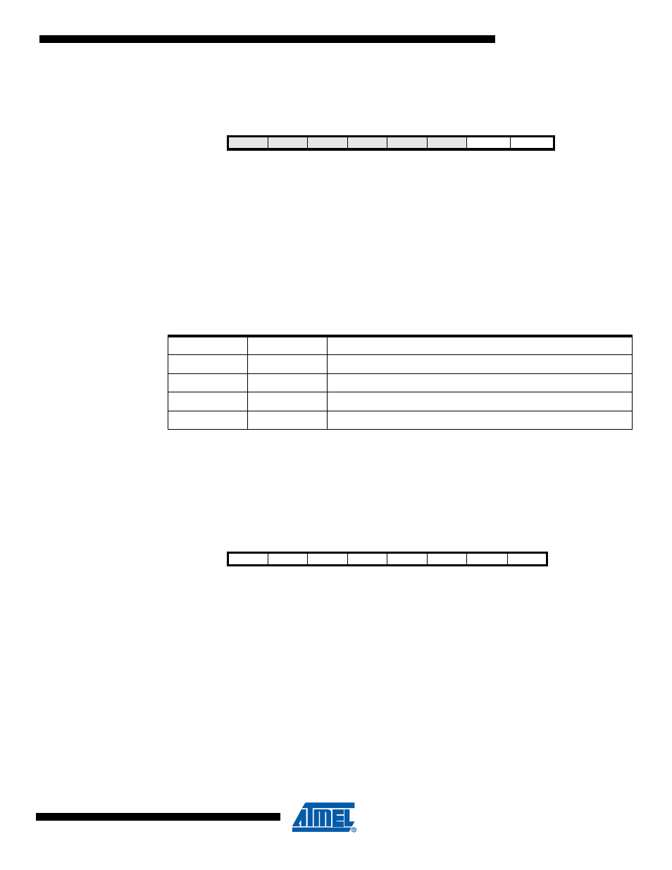
Bit
7
6
5
4
3
2
1
0
0x37
–
–
–
–
–
–
CLKMS1
CLKMS0
CLKMSR
Read/Write
R
R
R
R
R
R
R/W
R/W
Initial Value
0
0
0
0
0
0
0
0
Table 6-3.
Selection of Main Clock
CLKM1
CLKM0
Main Clock Source
0
0
Calibrated Internal 8 MHzOscillator
0
1
Internal 128 kHz Oscillator (WDT Oscillator)
1
0
External clock
1
1
Reserved
Bit
7
6
5
4
3
2
1
0
0x39
CAL7
CAL6
CAL5
CAL4
CAL3
CAL2
CAL1
CAL0
OSCCAL
Read/Write
R/W
R/W
R/W
R/W
R/W
R/W
R/W
R/W
Initial Value
0
0
0
0
0
0
0
0