4 pcicr – pin change interrupt control register, 5 pcifr – pin change interrupt flag register, 6 pcmsk – pin change mask register – Rainbow Electronics ATtiny10 User Manual
Page 39
39
8127B–AVR–08/09
ATtiny4/5/9/10
9.3.4
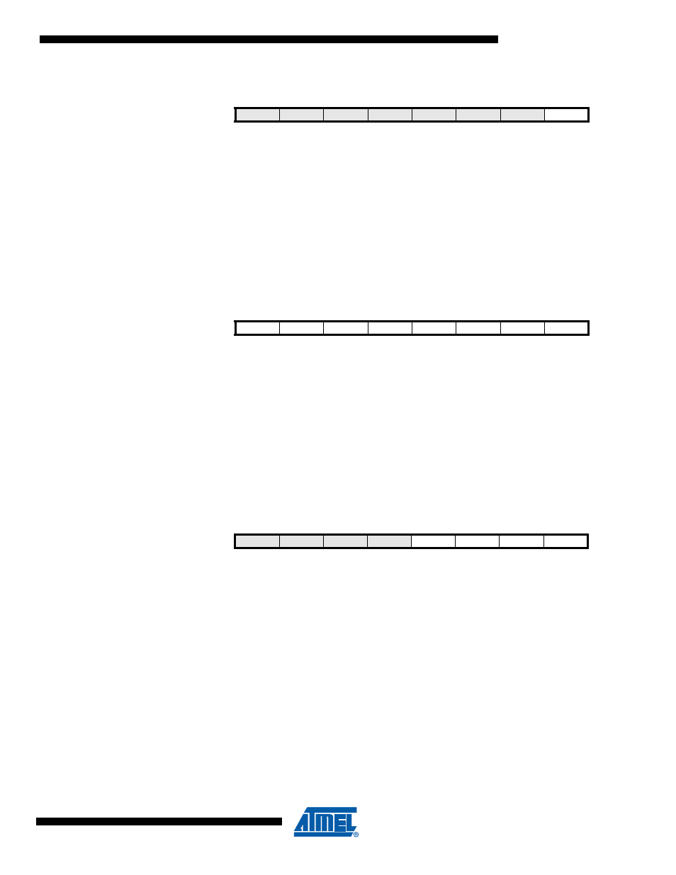
PCICR – Pin Change Interrupt Control Register
• Bits 7:1 – Res: Reserved Bits
These bits are reserved and will always read zero.
• Bit 0 – PCIE0: Pin Change Interrupt Enable 0
When the PCIE0 bit is set (one) and the I-bit in the Status Register (SREG) is set (one), pin
change interrupt 0 is enabled. Any change on any enabled PCINT3..0 pin will cause an interrupt.
The corresponding interrupt of Pin Change Interrupt Request is executed from the PCI0 Inter-
rupt Vector. PCINT3..0 pins are enabled individually by the PCMSK Register.
9.3.5
PCIFR – Pin Change Interrupt Flag Register
• Bits 7:1 – Res: Reserved Bits
These bits are reserved and will always read zero.
• Bit 0 – PCIF0: Pin Change Interrupt Flag 0
When a logic change on any PCINT3..0 pin triggers an interrupt request, PCIF0 becomes set
(one). If the I-bit in SREG and the PCIE0 bit in PCICR are set (one), the MCU will jump to the
corresponding Interrupt Vector. The flag is cleared when the interrupt routine is executed. Alter-
natively, the flag can be cleared by writing a logical one to it.
9.3.6
PCMSK – Pin Change Mask Register
• Bits 7:4 – Res: Reserved Bits
These bits are reserved and will always read zero.
• Bits 3:0 – PCINT3..0: Pin Change Enable Mask 3..0
Each PCINT3..0 bit selects whether pin change interrupt is enabled on the corresponding I/O
pin. If PCINT3..0 is set and the PCIE0 bit in PCICR is set, pin change interrupt is enabled on the
corresponding I/O pin. If PCINT3..0 is cleared, pin change interrupt on the corresponding I/O pin
is disabled.
Bit
7
6
5
4
3
2
1
0
0x12
–
–
–
–
–
–
–
PCIE0
PCICR
Read/Write
R
R
R
R
R
R
R
R/W
Initial Value
0
0
0
0
0
0
0
0
Bit
7
6
5
4
3
2
1
0
–
–
–
–
–
–
–
PCIF0
PCIFR
Read/Write
R
R
R
R
R
R
R
R/W
Initial Value
0
0
0
0
0
0
0
0
Bit
7
6
5
4
3
2
1
0
0x10
–
–
–
–
PCINT3
PCINT2
PCINT1
PCINT0
PCMSK
Read/Write
R
R
R
R
R/W
R/W
R/W
R/W
Initial Value
0
0
0
0
0
0
0
0