Comtech EF Data CDM-700 User Manual
Page 135
CDM-700 High Speed Satellite Modem
Revision 5
Clock Modes
MN/CDM700.IOM
8.2
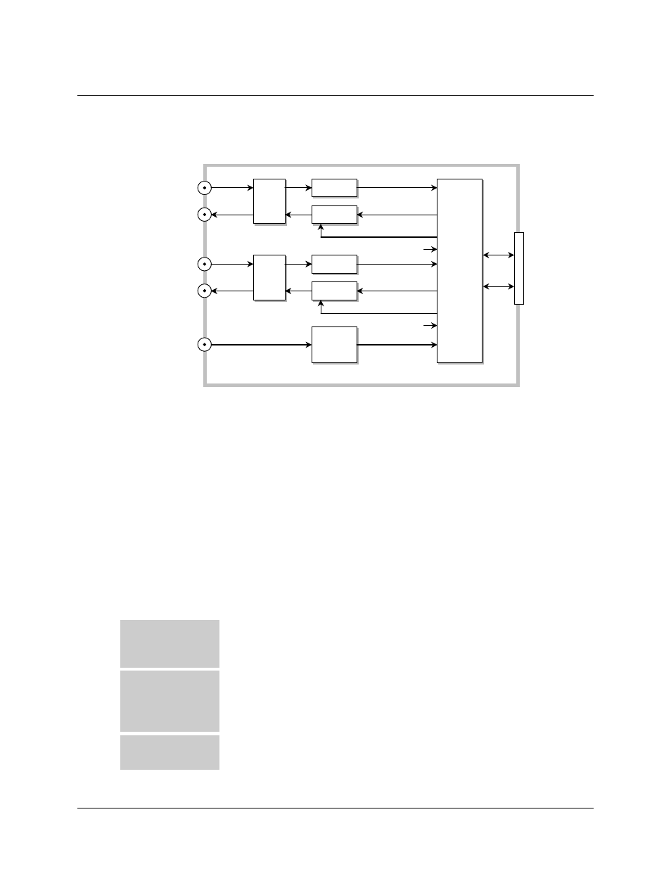
CDI-10 Dual G.703 Interface
The CDI-10 Dual G.703 interface has two ports that operate independently at an E3, T3, or STS-1
data rate. A port is a Tx/Rx pair. Figure 8-2 shows the interface.
Figure 8-2. CDI-10 G.703 Dual G.703 Interface
8.2.1 CDI-10 Dual G.703 Interface Transmit Clocking
For the G.703 interface, the only clock allowed is the SD signal applied to the Tx input. Internal
Clock and Rx Loop-Timed operation do not apply to G.703 applications.
8.2.2 CDI-10 Dual G.703 Interface Receive Clocking
When the Rx Buffer is disabled, the receive clock is the Rx-Sat. In this mode, ensure the Rx
Buffer is set to minimum to reduce latency.
When the Rx Buffer is enabled, the Rx clock selections are as follows:
Rx-Sat (default)
Selecting this clock disables the Rx Buffer because the input and output
clocks are both Rx-Sat. Normally, the Rx Buffer is set for minimum when
Rx-Sat is selected.
Tx-Terr
Uses the clock from the Tx input (SD) to clock out the Rx Buffer. The Tx
and Rx data rates are the same on this interface, so asymmetrical data
rates where Tx
≠ Rx is not permitted. The two data ports are independent,
so Port 1 may have a different data rate than Port 2.
Ext-Clk
Derives a clock from a signal input to the Ext-Clk connector on the
E3/T3/STS-1 Interface Module, not J7 on the modem.
Port 1
UNBAL
Port 1
UNBAL
Tx PLL
Tx PLL
Ext
BAL
Clock
Ext
BAL
Clock
Processor
Mux /
Demux
PLLs
Rx
Buffers
Interface
Loopback
Processor
Mux /
Demux
PLLs
Rx
Buffers
Interface
Loopback
Modem
Interface
Tx
Rx
Clk
&
Data
μC
BNC Female
5 Places
J3
J2
Dual E3/T3/STS-1 Card
Loopback
EXT Clk
J1
External Clock
Rx Buffer
Rx Buffer
Rx Buffer Clk
Port 2
UNBAL
Port 2
UNBAL
Tx PLL
Tx PLL
Tx
Rx
J5
J4
Rx Buffer
Rx Buffer
Rx Buffer Clk
Loopback
Port 1
Port 2
SD
RD
SD
RD
8–3