2 post code register, 3 super io configuration register, Table 6-10 – Artesyn ATCA 7370 / ATCA 7370-S Installation and Use (January 2015) User Manual
Page 125: Post code register, Table 6-11, Super i/o configuration index register, Table 6-12, Super i/o configuration data register, Maps and registers
Maps and Registers
ATCA-7370/ATCA-7370-S Installation and Use (6806800P54H)
125
6.2.2
POST Code Register
The FPGA provides an 8-bit wide register to store POST codes to the LPC I/O address 0x80.
The IPMC may read the POST code using the SPI interface (with the signal BMC_SPI_S0_N
asserted) and the SPI address 0x7F.
6.2.3
Super IO Configuration Register
After a LPC reset (ICH_PLTRST_ is asserted) or "Power On Reset" the Super IO is in the run mode
with the UARTs disabled. They may be configured using the LPC IO address range SIW (INDEX
and DATA) by placing the Super IO into configuration mode. The BIOS uses these configuration
addresses to initialize the logical devices at POST. The INDEX and DATA addresses are only valid
when the Super IO is in configuration state. The INDEX and DATA addresses are effective only
when the Super IO is in the configuration state. When the Super IO is not in the configuration
state, reads return 0xFF and write data is ignored.
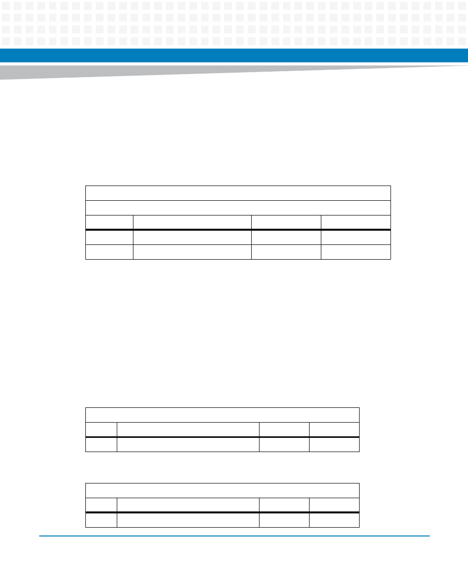
Table 6-10 POST Code Register
LPC I/O Address: 0x80
IPMC SPI Address: 0x7f
Bit
Description
Default
Access
7:0
POST codes from host
0
LPC: r/w
IPMC: r
Table 6-11 Super I/O Configuration Index Register
LPC I/O Address: 0x4E
Bit
Description
Default
Access
7:0
INDEX. Configuration Index.
0xff
LPC: r/w
Table 6-12 Super I/O Configuration Data Register
LPC I/O Address: 0x4F
Bit
Description
Default
Access
7:0
DATA Configuration Data.
0xff
LPC: r/w