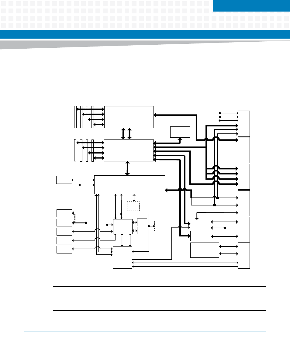
Functional description, 1 block diagram, Figure 5-1 – Artesyn ATCA 7370 / ATCA 7370-S Installation and Use (January 2015) User Manual
Page 103: Block diagram, Chapter 5
Chapter 5
ATCA-7370/ATCA-7370-S Installation and Use (6806800P54H)
103
Functional Description
5.1
Block Diagram
Note: On the single processor variant the processor and its DIMM sockets are populated on
the upper side of the board. Components associated with the second processor are not
populated on this product variant.
Figure 5-1
Block Diagram
Patsburg-B
PCH
82599
Dual 10GbE
Powerville
Quad GbE
Dual GbE-T (P2/3, Base)
FPGA
H8S
On-board Power
Supplies & Hot
Swap Circuitry
Zone1
to
Back
plane
P10
2x USB
Serial
Console
EFI
FW
EFI
FW
LPC
SPI
IPMB-A
IPMB-B
-48V
-48V
COM1
2x USB
SATA
QPI
Zone3
to
RTM
J30
Control, Power
COM2
COM2
1x USB
1x USB
SANDY BRIDGE-EP 0#
SANDY BRIDGE-EP 1#
TPM
DMI2
PCIe x8, Port3a,b
Reset
Button
Dual GbE-T (P0/1)
(optional)
PCIe x1
4x SAS 2.0
SPI
1000
Base-T
ATCA-7370-0GB
Zone3
to
RTM
J31
Zone3
to
RTM
J32
Zone2
to
Back
plane
J23
Zone2
to
Back
plane
J20
Dual 1/10GbE-X (Fabric)
2xUSB
SPI
4 DDR3 VLP DIMM Slots
4 DDR3 VLP DIMM Slots
SMB
SPI
PCIe x16 / Dual x8 / Quad x4, Port2a,b,c,d
2x SAS (UC1/2)
2x SAS
1000
Base-T
Dual GbE-T (P0/1)
PCIe x4
PCIe x4
PCIe x16
PCIe x4, Port1b
MO297
SSD
(optional)
(optional)
PCIe x4, Port1a
2x SAS (UC3/4)
PCIe x4
PCIe x4
PCIe x4
(optional)
2x SAS
Handle
Switch
1x GbE-X (P0, UC0)
PCIe x8 / Dual x4, Port3c,d
PCIe x16, Port2a,b,c,d
COM3
PCIe
Connector