2 spi register decoding, Table 6-8, Lpc i/o register map overview – Artesyn ATCA 7370 / ATCA 7370-S Installation and Use (January 2015) User Manual
Page 124: Table 6-9, Ipmc spi register, Maps and registers
Maps and Registers
ATCA-7370/ATCA-7370-S Installation and Use (6806800P54H)
124
6.2.1.1.1 LPC I/O Decoding
The LPC interface responds to LPC I/O accesses listed in the
. All other LPC I/O accesses
are ignored.
All LPC I/O accesses to the address range REGISTERS are decoded by the LPC core.
6.2.1.1.2 LPC Memory Decoding
The LPC interface never responds to LPC memory accesses.
6.2.1.1.3 LPC Firmware Decoding
The LPC interface never responds to LPC firmware accesses.
6.2.1.2
SPI Register Decoding
All SPI accesses from the IPMC towards the FPGA with the SPI select signal BMC_SPI_S0_N
asserted are for the internal registers.
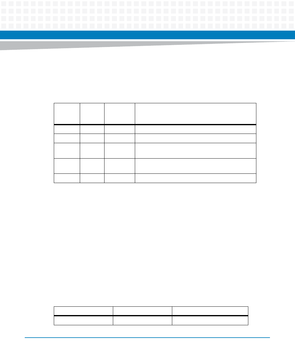
Table 6-8 LPC I/O Register Map Overview
Base
Address
Address
Size
Address
Range
Name
Description
0x4E
2
SIW
Super IO Configuration Registers for Index and Date
0x80
1
POSTCODE
POST Code Register
BASE1
8
COM1
UART1. Serial Port 1 (Logical Device 4). BASE1 address is
set up during Super IO Configuration.
BASE2
8
COM2
UART2. Serial Port 2. (Logical Device 4). BASE2 address is
set up during Super IO Configuration.
0x600
128
REGISTERS
FPGA Registers
Table 6-9 IPMC SPI Register
SPI Address Range
Address Range Name
Description
0x00 - 0x7F
REGISTERS
FPGA Registers