3 cf connector, Figure 4-30: cf connector, Figure 4-31: compactflash® reference design – IEI Integration ICE-DB-9S User Manual
Page 81: Ice module page 68, Cf connector
ICE Module
Page 68
Notes: When using a 44- pin IDE connector, pins 41 and 42 must be connected to VCC
and pins 43 and 44 must be connected to ground. All other pins are equivalent to a
40-pin IDE connector. Additionally, decoupling capacitors should be connected to the
VCC pins.
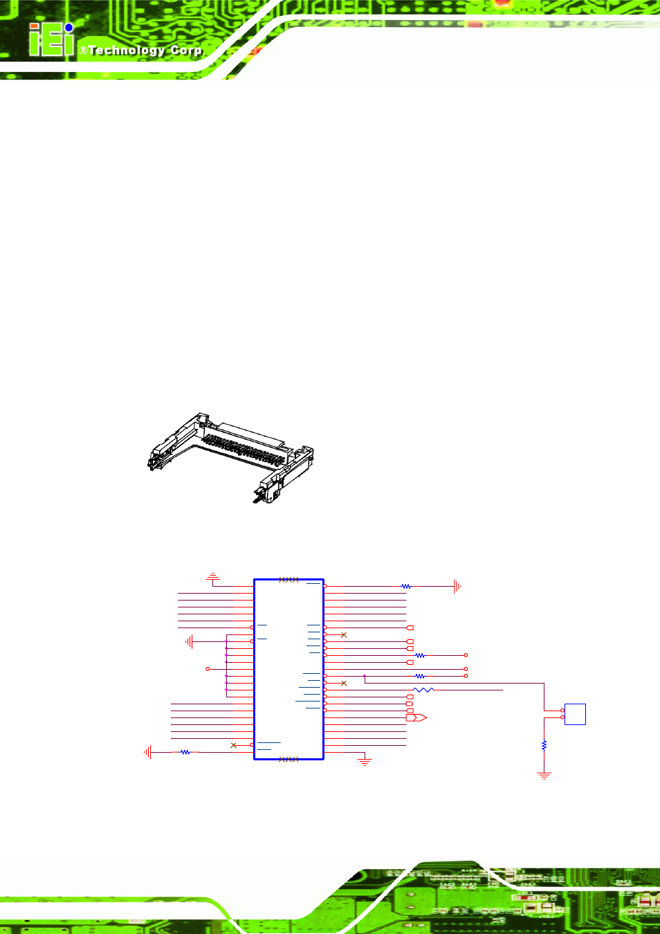
4.9.3 CF Connector
CompactFlash (CF) cards with DMA capability require that the two signals 'IDE_REQ'
and 'IDE_ACK#' are routed to the CF card socket on the COM Express carrier board.
If this is not done then some DMA capable CF cards may not work because they are
not designed for non DMA mode. For more information about this subject refer to the
datasheet of the CF card or contact your CF card manufacturer. If two CF cards are
used in master/slave mode on the same IDE channel, the signal 'CSEL#' of the CF
card socket that drives the slave CF card must be tied to ground. In master mode the
'CSEL#' signal must be left open. Figure 4-31 shows a circuitry implementing a CF
card socket that is DMA capable.
Figure 4-30: CF Connector
IDE_D4
IDE_D2
IDE_D0
IDE_IRQ
3
IDE_ACK#
3
IDE_REQ
3
IDE_IOW#
3
IDE_IOR# 3
IDE_IORDY
3
R139
33_4
1
2
IDE_D8
IDE_D13
IDE_D14
IDE_D11
IDE_D12
IDE_D9
IDE_D10
IDE_D15
IDE_D3
IDE_D1
HDD_LED# 20,21
IDE_D5
IDE_D7
IDE_D6
IDE_RESET#
IDE_CS#3
3
CF Connector
R141
1K_4
JCF1
HEADER 2
1
1
2
2
IDE_CBLID#
IDE_SDA2
+V5
IDE_SDA0
IDE_SDA1
R136
10K_4
+V5
CF1
CFIIB-SMD
GND1
1
D3
2
D4
3
D5
4
D6
5
D7
6
CE
7
A10
8
OE
9
A9
10
A8
11
A7
12
VCC1
13
A6
14
A5
15
A4
16
A3
17
A2
18
A1
19
A0
20
D0
21
D1
22
D2
23
IOCS16
24
CD2
25
CD1
26
D11
27
D12
28
D13
29
D14
30
D15
31
CE2
32
VS1
33
IOR
34
IOW
35
WE
36
IRQ
37
VCC2
38
CSEL
39
VS2
40
RESET
41
WAIT
42
INPACK
43
REG
44
BVD2
45
BVD1
46
D8
47
D9
48
D10
49
GND2
50
51
51
52
52
53
53
54
54
55
55
56
56
R142
100_4_1%
+V5
R131
100_4_1%
R133
10K_4
IDE_CS#1
+V5
JCF1
SHORT : MASTER
OPEN : SLAVE
Figure 4-31: CompactFlash® Reference Design