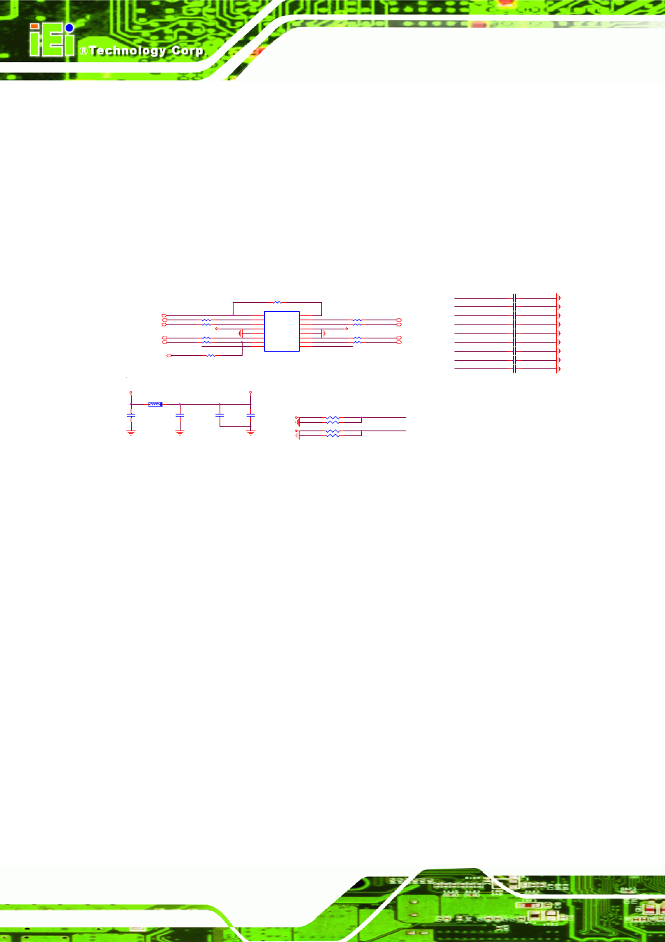
4 pci clock buffer, 5 pci routing guideline, Figure 4-16: pci clock buffer example – IEI Integration ICE-DB-9S User Manual
Page 63: Pci clock buffer
ICE Module
Page 50
4.3.4 PCI Clock Buffer
The COM Express Specification only supports a single PCI clock signal called
'PCI_CLK'
to be used on the carrier board. If there are multiple devices or slots
implemented on the carrier board, a zero delay clock buffer is required to expand the
number of PCI clocks so that each device or each bus slot will be provided with a
separate clock signal.
CLK33M_MINICARD 5
U2
CY 2309NZSXC-1H
REF
1
CLKA1
2
CLKA2
3
VDD
4
GND
5
CLKB1
6
CLKB2
7
S2
8
S1
9
CLKB3
10
CLKB4
11
GND
12
VDD
13
CLKA3
14
CLKA4
15
CLKOUT
16
CLK33M_SLOT3
CLK33M_BIOS2
C265
10P_4_N_50V
1
2
CLK33M_SLOT1 7
CLK33M_SLOT2 7
CLKBUFFER_S2
CLKBUFFER_S1
C17
0.1U_4_Y_16V
C16
10U_8_X_6V3
C18
0.1U_4_Y_16V
C15
10U_8_X_6V3
+V3.3
FB3
FB30_8_3A
CLK33M_80PORT
C14
10P_4_N_50V
1
2
CLK33M_BIOS2
20
+V3.3_CLKBUFFER
CLK33M_TPM
C266
10P_4_N_50V
1
2
+V3.3_CLKBUFFER
C13
10P_4_N_50V
1
2
PCI Clock Buffer
+V3.3_CLK
R65
10K_4
1
2
CLKBUFFER_S2
R67
@10K_4
1
2
R62
10K_4
1
2
CLKBUFFER_S1
+V3.3_CLK
R63
@10K_4
1
2
CLK33M_PCI
3
C10
10P_4_N_50V
1
2
CLK33M_SLOT1
CLK33M_SLOT3
7
R45
33_4
1
2
CLK33M_SIO2
C241
10P_4_N_50V
1
2
CLK33M_MINICARD
C11
10P_4_N_50V
1
2
C267
10P_4_N_50V
1
2
V1.01 Modify
CLK33M_MINIPCI
8
R37
33_4
1
2
R40
33_4
1
2
CLK33M_MINIPCI
C12
10P_4_N_50V
1
2
R38
33_4
1
2
R41
33_4
1
2
R34
@33_4
1
2
CLK33M_SIO2 14
CLK33M_TPM
11
R51
33_4
1
2
CLK33M_SLOT2
CLK33M_80PORT
9
R44
33_4
1
2
R47
33_4
1
2
+V3.3_CLKBUFFER
R48
33_4
1
2
Figure 4-16: PCI Clock Buffer Example
4.3.5 PCI Routing Guideline
Particular attention must be paid to the PCI clock routing. The PCI Local Bus
specification requires a maximum propagation delay for the clock signals of 10ns
within a propagation skew of 2ns @ 33MHz between the several clock signals. The
COM Express Specification allows 1.6ns ± 0.1ns @ 33MHz propagation delay for the
PCI clock signal beginning from the module pin to the destination pin of the PCI device.
The propagation delay is dependent on the trace geometries, PCB stack-up and the
PCB dielectric constant. Calculating using a typical propagation delay value of
180ps/inch for an internal layer clock trace of the carrier board, a maximum trace
length of 8.88 inches is allowed.
The clock trace from the COM Express module to a PCI bus slot should be 2.5 inches
shorter because PCI cards are specified to have 2.5 inches of clock trace length on
the card itself. PCI clock signals should be routed as a single ended trace with a trace
impedance of 55Ω. To reduce EMI, a single ground referenced internal layer is
recommended. The clock traces should be separated as far as possible from other