6 pci express routing guideline, 1 impedance consideration, Table 4-4: pci express impedance consideration – IEI Integration ICE-DB-9S User Manual
Page 48
Page 35
ICE Module
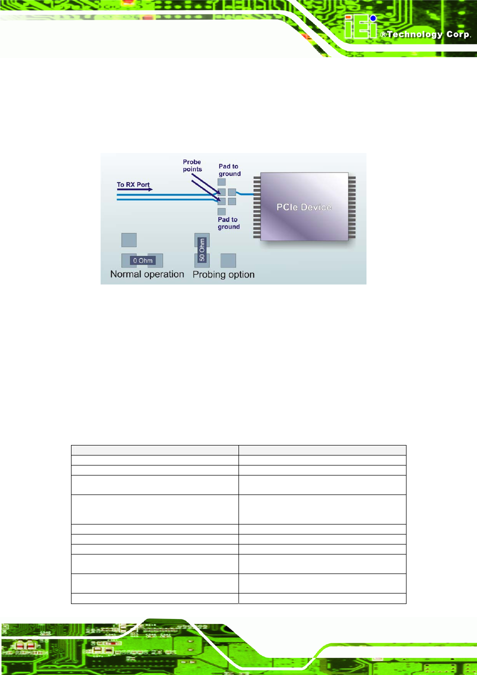
be as small as possible, preferably 0402. To enable the test mode, a 50 Ω ±1%
resistor stuffing option is needed to break the path. This will force the transmitter port
to enter the compliance mode and begin transmitting the compliance packet.
Otherwise, use a 0-Ω resistor to continue the trace route to the Rx port. This will allow
normal operation of the device.
Figure 4-2: Intel Recommend Test Structure for PCI Express Data Eye Measurement
4.1.6 PCI Express Routing Guideline
4.1.6.1 Impedance Consideration
The PCI Express impedance considerations are listed in Table 4-4.
Table 4-4: PCI Express Impedance Consideration
Parameters
Routing
Transfer Rate / PCIe Lane
2.5 Gbits/sec
Maximum signal line length (coupled traces) TX and RX path: 21.0 inches
Maximum signal length allowance on the
COM Express module "
TX and RX path: 5.15 inches
Signal length allowance on the COM
Express carrier board "
TX and RX path: 15.85 inches @
0.28dB/GHz/inch to PCIe device 9.00 inches
@ 0.28dB/GHz/inch to PCIe slot
Differential Impedance
100 Ohms +/-20%
Single-ended Impedance
55 Ohms +/-15%
Trace width (W)
5 mils (microstrip routing) (*)
Spacing between differential pairs (intra-pair)
(S)
4 mils (microstrip routing) (*)
Spacing between RX and TX pairs
(inter-pair) (s)
Min. 20mils
Spacing between differential pairs and
Min. 50mils