3 pci, 1 signal description, Table 4-8: pci signal description – IEI Integration ICE-DB-9S User Manual
Page 60
Page 47
ICE Module
4.3 PCI
The COM Express provides a PCI Bus interface that is compliant with the PCI Local
Bus Specification,
Revision 2.2. The implementation is optimized for high-performance
data streaming when the COM Express is acting as either the target or the initiator on
the PCI bus. For more information on the PCI Bus interface, refer to the PCI Local Bus
Specification,
Revision 2.2.
4.3.1 Signal Description
Table 4-8 shows COM Express PCI bus signal, including pin number, signals, I/0,
power plane, terminal resistors, damping resistors and descriptions.
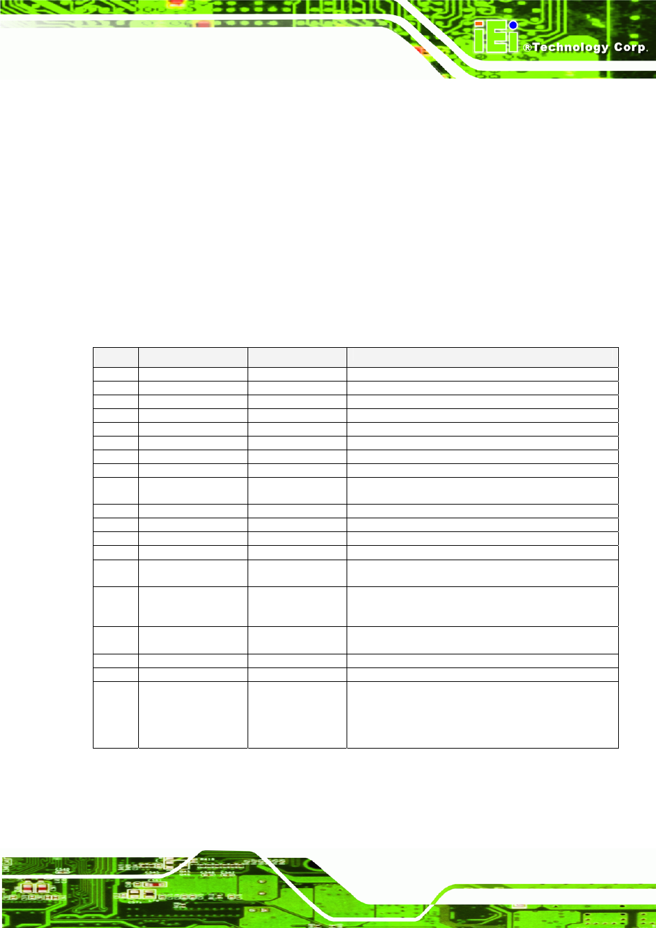
Table 4-8: PCI Signal Description
Pin
Signal
I/O
Description
Note1 PCI_AD[0..31]
I/O 3.3V
PCI bus multiplexed address and data lines
Note1 PCI_C/BE[0..3]#
I/O 3.3V
PCI bus byte enable lines , active low
C36
PCI_DEVSEL#
I/O 3.3V
PCI bus Device Select, active low.
D36
PCI_FRAME#
I/O 3.3V
PCI bus Frame control line, active low.
C37
PCI_IRDY#
I/O 3.3V
PCI bus Initiator Ready control line, active low.
D35
PCI_TRDY#
I/O 3.3V
PCI bus Target Ready control line, active low.
D34
PCI_STOP#
I/O 3.3V
PCI bus STOP control line, active low.
D32
PCI_PAR
I/O 3.3V
PCI bus parity
C34
PCI_PERR#
I/O 3.3V
Parity Error: An external PCI device drives PERR# to
low, when it receives data that has a parity error.
Note1 PCI_REQ[0..3]#
I 3.3V
PCI bus master request input line, active low.
Note1 PCI_GNT[0..3]#
O 3.3V
PCI bus master grant output lines, active low.
C23
PCI_RESET#
O 3.3V
PCI Reset output, active low.
C35
PCI_LOCK#
I/O 3.3V
PCI Lock control line, active low.
D33
PCI_SERR#
I/O 3.3V
System Error: SERR# may be pulsed active by any
PCI device that detects a system error condition.
C15
PCI_PME#
I 3.3VSB
PCI Power Management Event: PCI peripherals drive
PME# to low to wake up the system from low-power
states S1–S5.
D48
PCI_CLKRUN#
I/O 3.3V
Bidirectional pin used to support PCI clock run
protocol for mobile systems.
Note1 PCI_IRQ[A..D]#
I
3.3V
PCI interrupt request lines.
D50
PCI_CLK
O 3.3V
PCI 33MHz clock output.
D49
PCI_M66EN
I 3.3V
Module input signal that indicates whether an carrier
board PCI device is capable of 66MHz operation. It is
pulled to ground by carrier board device or by slot
card, if one of the devices are NOT capable of
66MHz operation.
Please refer to Table 3-3: Module Type 2 Connector Pinout Rows (A and B) or
Table 3-4: Module Type 2 Connector Pinout Rows (C and D)
.