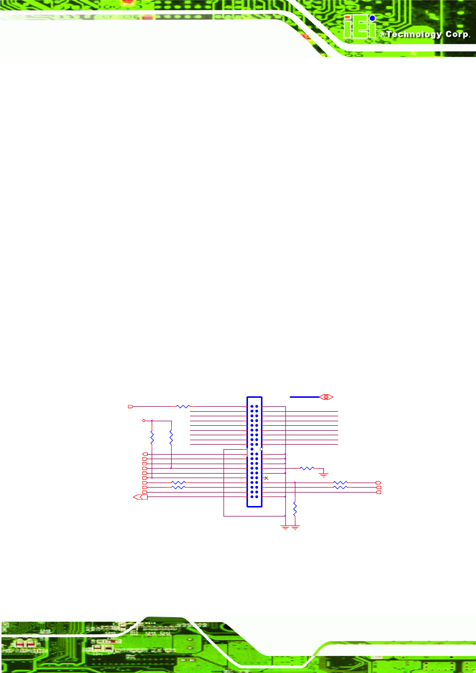
2 ide connector, Figure 4-29: ide reference design, Ide connector – IEI Integration ICE-DB-9S User Manual
Page 80: Page 67 ice module

Page 67
ICE Module
D10 IDE_ACK#
O 3.3V
IDE device DMA acknowledge.
D16 IDE_CS1#
O 3.3V
IDE device chip select for 1F0h to 1FFh range.
D17 IDE_CS3#
O 3.3V
IDE device chip select for 3F0h to 3FFh range.
C13 IDE_IORDY
I 3.3V
IDE device I/O ready input. Pulled low by the IDE device to
extend the cycle.
D18 IDE_RESET#
O 3.3V
Reset output to IDE device, active low.
D12 IDE_IRQ
I 3.3V
Interrupt request from IDE device.
D77 IDE_CBLID#
I 3.3V
Input from off-module hardware indicating the type of IDE
cable being used. High indicates a 40-pin cable used for
legacy IDE modes. Low indicates that an 80-pin cable with
interleaved grounds is used. Such a cable is required for
Ultra-DMA 66, 100 modes.
4.9.2 IDE Connector
To interface standard 3.5-inch parallel ATA drives, a standard 2.54mm, two row,
40-pin connector in combination with a ribbon conductor cable is used. For slower
drive speeds up to ATA33, a normal 40-pin, 1.0mm-pitch conductor cable is sufficient.
Higher transfer rates like ATA66 and ATA100 require 80-pin conductor cables, where
the extra 40 conductors are tied to ground to isolate the adjacent signals for better
signal integrity. The signal 'IDE_CBLID#' of the COM Express carrier board indicates
which conductor cable is used. It ties to ground if a 80-pin conductor cable is
connected. This allows the module's BIOS to determine the maximum transfer rate
that can be driven and set up the proper drive parameters for the IDE controller.
IDE_A0
3
IDE_CS#1
3
IDE_CS#3
3
IDE_ACK#
3
IDE_REQ
3
IDE_IOW#
3
IDE_IRQ
3
IDE_A2
3
IDE_IOR#
3
IDE_IORDY
3
PIDE1
BOXHEADER_2X20_2.54
1
2
3
4
5
6
7
8
9
10
11
12
13
14
15
16
17
18
19
21
22
23
24
25
26
27
28
29
30
31
32
33
34
35
36
37
38
39
40
20
R140
10K_4
1
2
R132
470_4
IDE_D12
IDE_D9
IDE_D10
IDE_D8
IDE_D15
IDE_D14
IDE_D11
IDE_D13
IDE_SDA2
R135
0_4
1
2
R134
33_4
1
2
IDE_CBLID#
3
R138
33_4
1
2
IDE_SDA1
HDD_LED#
20,21
R129
8.2K_4
R130
4.7K_4
1
2
IDE_D6
IDE_D2
IDE_D5
IDE_D7
IDE_D1
IDE_D0
IDE_D3
IDE_D4
R128
33_4
1
2
+V3.3
R137
33_4
1
2
IDE_D[15..0] 3
IDE Connector
IDE_RESET#
3
IDE_SDA0
IDE_A1
3
Figure 4-29: IDE Reference Design
