2 pci connector, 3 pci irq assignment, Figure 4-14: pci slot connection example – IEI Integration ICE-DB-9S User Manual
Page 61: The pci slot connection is show n in figure 4-14
ICE Module
Page 48
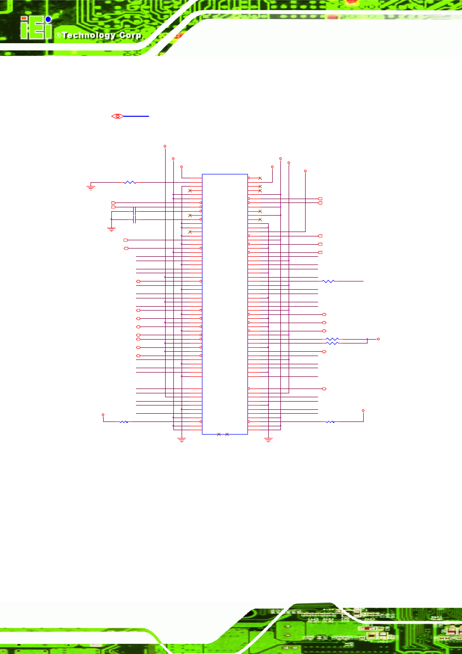
4.3.2 PCI Connector
The PCI slot connection is shown in Figure 4-14.
+V3.3
+V12
R81
10K_4
+V3.3
PCI_AD20
R83
10K_4
R79
100_4_1%
1
2
+V5
PCI_AD10
PCI_AD3
PCI_AD25
PCI_AD19
PCI_AD12
PCI_AD29
PCI_AD17
PCI_AD21
PCI_AD7
PCI_AD5
PCI_AD23
PCI_AD1
PCI_AD31
PCI_AD27
PCI_AD14
PCI_AD8
PCI1
PCISLOT120_2.54
-12V
B1
TCK
B2
GND11
B3
TDO
B4
+5V07
B5
+5V08
B6
INTB#
B7
INTD#
B8
PRSNT1#01
B9
RSVD03
B10
PRSNT1#02
B11
GND12
B12
GND13
B13
RSVD04
B14
GND14
B15
CLK
B16
GND15
B17
REQ#
B18
+5V09
B19
AD31
B20
AD29
B21
GND16
B22
AD27
B23
AD25
B24
+3.3V07
B25
C/BE3#
B26
AD23
B27
GND17
B28
AD21
B29
AD19
B30
+3.3V08
B31
AD17
B32
C/BE2#
B33
GND18
B34
IRDY#
B35
+3.3V09
B36
DEVSEL#
B37
GND19
B38
LOCK#
B39
PERR#
B40
+3.3V10
B41
SERR#
B42
+3.3V11
B43
C/BE1#
B44
AD14
B45
GND20
B46
AD12
B47
AD10
B48
GND21
B49
AD8
B52
AD7
B53
+3.3V12
B54
AD5
B55
AD3
B56
GND22
B57
AD1
B58
+5V10
B59
ACK64#
B60
+5V11
B61
+5V12
B62
TRST#
A1
+12V
A2
TMS
A3
TDI
A4
+5V01
A5
INTA#
A6
INTC#
A7
+5V02
A8
RSVD
A9
+5V03
A10
RSVD02
A11
GND01
A12
GND02
A13
3.3VAUX
A14
RST#
A15
+5V04
A16
GNT#
A17
GND03
A18
PME#
A19
AD30
A20
+3.3V01
A21
AD28
A22
AD26
A23
GND04
A24
AD24
A25
IDSEL
A26
+3.3V02
A27
AD22
A28
AD20
A29
GND05
A30
AD18
A31
AD16
A32
+3.3V03
A33
FRAME#
A34
GND06
A35
TRDY#
A36
GND07
A37
STOP#
A38
+3.3V04
A39
SMBCLK
A40
SMDATA
A41
GND08
A42
PAR
A43
AD15
A44
+3.3V05
A45
AD13
A46
AD11
A47
GND09
A48
AD9
A49
C/BE0#
A52
+3.3V06
A53
AD6
A54
AD4
A55
GND10
A56
AD2
A57
AD0
A58
+5V05
A59
REQ64#
A60
+5V
A61
+5V06
A62
X1
X1
X
2
X
2
R85
8.2K_4
+V5
+V5
R86
8.2K_4
PCI_AD15
PCI_AD11
PCI_AD18
PCI_AD0
PCI_AD6
PCI_AD9
PCI_AD22
PCI_AD26
PCI_AD4
PCI_AD28
PCI_AD30
PCI_AD16
PCI_AD20
PCI_AD2
PCI_AD13
PCI_AD24
C50
0.1U_4_Y_16V
C51
0.1U_4_Y_16V
R77
5.6K_4
1
2
+V3.3_DUAL
-V12
PCI_FRAME# 3,8,9
PCI_C/BE#2
3,8,9
PCI_C/BE#0
3,8,9
PCI_C/BE#1
3,8,9
PCI_C/BE#3
3,8,9
PCI_RST# 3,8,9,13
PCI_PAR
3,8
PCI_SERR#
3,8
PCI_STOP#
3,8
PCI_TRDY#
3,8
PCI_IRDY#
3,8,9
PCI_DEVSEL#
3,8
PCI_LOCK#
3
PCI_INT#A 3,8
PCI_INT#B
3,8
PCI_INT#D
3
PCI_INT#C
3
+V5
CLK33M_SLOT1
4
+V3.3
PCI_PME#
PCI_PME#
3,8
PCI_AD[0..31]
3,8,9
PCI_PERR#
3,8
PCI_GNT#1 3
PCI_REQ#1
3
Figure 4-14: PCI Slot Connection Example
4.3.3 PCI IRQ Assignment
Most of this PCI devices only utilize the interrupt signal 'INTA#'. To distribute the
interrupt source of the devices over the interrupt signals 'INTB#', 'INTC#' and 'INTD#',
an interrupt cross routing has to be implemented on the COM Express carrier board
design. Figure 5-14 and Table 5-16 illustrate the PCI bus interrupt routing for the PCI
bus slots 1-4. The PCI REQ and GNT lines with the same index must be considered