2 digital and analog signals isolation, 3 emi consideration, 9 ide – IEI Integration ICE-DB-9S User Manual
Page 79: 1 signal description, Figure 4-28: audio analog power example, Table 4-18: ide signals description, Ice module page 66

ICE Module
Page 66
+V5_AUDIO
EC12
100U_SMD6_3_EC_25V
FB9
FB_80_6_600MA
1
2
C188
0.1U_4_Y_16V
Q9
GS78L05N_TO92_3
TO92_123
VOUT
1
VIN
3
GND
2
+V12
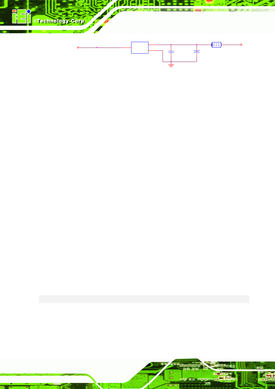
Figure 4-28: Audio Analog Power Example
4.8.1.2 Digital and Analog Signals Isolation
Analog audio signals and other digital signals should be routed as far as possible from
each other. All audio circuits require careful PCB layout and grounding to avoid picking
up digital noise on audio-signal lines.
4.8.1.3 EMI Consideration
Any signals entering or leaving the analog area must cross the ground split in the area
where the analog ground is attached to the main motherboard ground. That is, no
signal should cross the split/gap between the ground planes, which would cause a
ground loop, thereby greatly increasing EMI emissions and degrading the analog and
digital signal quality.
4.9 IDE
Type 2 and 4 COM Express modules provide a single channel IDE interface
supporting two standard IDE hard drives or ATAPI devices with a maximum transfer
rate of ATA100 (Ultra-DMA-100 with 100MB/s transfer rate). The corresponding
signals can be found on the module connector rows C and D.
4.9.1 Signal Description
Table 4-18 shows COM Express PCI IDE signals, including pin number, signals, I/0,
power plane, terminal resistors, damping resistors and descriptions.
Table 4-18: IDE signals description
Pin
Signal
I/O
Description
IDE_D[0..15]
I/O 3.3V
Bidirectional data to / from IDE device.
D13
D14
D15
IDE_A[0:2]
O 3.3V
Address lines to IDE device.
D9
IDE_IOW#
O 3.3V
I/O write line to IDE device.
C14 IDE_IOR#
O 3.3V
I/O read line to IDE device.
D8
IDE_REQ
I 3.3V
IDE device DMA request. It is asserted by the IDE device
to request a data transfer.
